MDDR Subsystem
Microsemi Proprietary UG0446 User Guide Revision 7.0
68
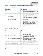
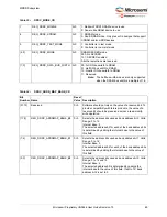
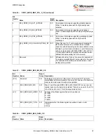
[31:15]
Reserved
0×0
Software should not rely on the value of a reserved bit.
To provide compatibility with future products, the value of
a reserved bit should be preserved across a read-
modify-write operation.
[14:3]
REG_DDRC_T_RFC_NOM_X32
0×52
t
REFI
: Average time between refreshes (specification: 7.8
µs). Unit: multiples of 32 clocks.
[2:0]
REG_DDRC_REFRESH_BURST
0×0
The programmed value plus one is the number of refresh
timeouts that is allowed to accumulate before traffic is
blocked and the refreshes are forced to execute. Closing
pages to perform a refresh is a one-time penalty that
must be paid for each group of refreshes; therefore,
performing refreshes in a burst reduces the per-refresh
penalty of these page closings.
Higher numbers for burst_of_N_refresh slightly
increases utilization; lower numbers decreases the
worst-case latency associated with refreshes.
0x0: Single refresh
0x1: Burst-of-2
0x7: Burst-of-8 refresh
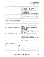
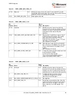
Table 32 •
DDRC_DYN_POWERDOWN_CR
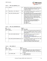
Bit
Number Name
Reset
Value Description
[31:2]
Reserved
0×0
Software should not rely on the value of a reserved bit.
To provide compatibility with future products, the value of
a reserved bit should be preserved across a read-modify-
write operation.
1
REG_DDRC_POWERDOWN_EN
0×1
If true, the controller goes into power-down after a
programmable number of cycles
(
This register bit may be reprogrammed during the course
of normal operation.
0
REG_DDRC_DEEPPOWERDOWN_EN 0×0
1: Controller puts the DRAM into deep power-down mode
when the transaction store is empty.
0: Brings controller out of deep power-down mode.
Present only in designs that have mobile support.
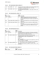
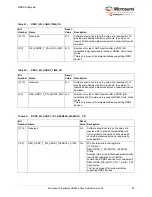
Table 33 •
DDRC_MODE_CR
Bit
Number
Name
Reset
Value
Description
[31:9]
Reserved
0×0
Software should not rely on the value of a reserved bit. To
provide compatibility with future products, the value of a
reserved bit should be preserved across a read-modify-write
operation.
8
REG_DDRC_DDR3
0×0
1: DDR3 operating mode
0: DDR2 operating mode
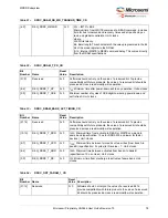
Table 31 •
DDRC_DYN_REFRESH_2_CR


