DDR Bridge
Microsemi Proprietary UG0446 User Guide Revision 7.0
216
5.4
DDR Bridge Control Registers in MDDR and FDDR
The following table lists HPMS DDR bridge control registers in the MDDR and FDDR. Refer to the
"MDDR Subsystem" chapter on page 5
"Fabric DDR Subsystem" chapter on page 134
for a
detailed description of each register and bit.
5.5
Appendix A: How to Use DDR Bridge in SmartFusion2
Device
This section describes how to use DDR Bridge in an application and contains the following sub-sections:
•
•
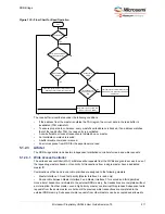
Use Model 1: High Speed Data Transactions from Cortex-M3 Processor
•
Use Model 2: Selecting Non-Bufferable Region
5.5.0.1
MSS DDR Bridge Configurations
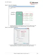
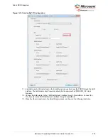
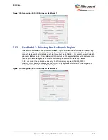
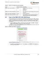
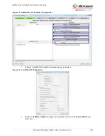
The MSS DDR bridge is statically configured through the DDR bridge configurator of the MSS
configurator in Libero SoC, as shown in the following image. Configurable parameters are as follows:
•
Write buffer time out counter
: This allows to configure the 10-bit timer of write buffer for time out
value. By default this is configured for maximum wait time (0×3FF) to buffer the write transactions.
For configuring to other values enter a 10-bit hexadecimal value in the provided field of DDR bridge
configurator. Select timeout value to a non zero value for buffering the write transactions.
•
Non-bufferable region size: The size of non-bufferable memory region can be selected from a drop-
down menu in the DDR bridge configurator. The menu has the options to select the region from 64
KB to 1 GB. It also has an option “none” to select the complete memory as bufferable. The default
selection is 64 KB.
•
Non-bufferable region address
: The base address of the non-bufferable memory region can be
selected by configuring this field. The value must be configured as a 16-bit hexadecimal address.
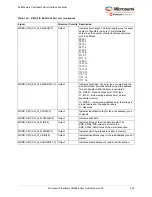
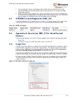
MSSDDR_FACC1_CR
RW-P
Field
CC_RESET_N HPMS DDR fabric alignment clock
controller 1 configuration register.
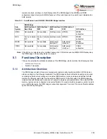
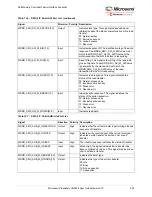
Table 165 •
DDR Bridge Control Registers in MDDR and FDDR
Register Name
Address
Offset
R/W
Reset
Source
Description
DDR_FIC_NB_ADDR_CR,
0×400
RW PRESET_N Indicates the base address of the non-
bufferable address region.
DDR_FIC_NBRWB_SIZE_CR,
0×404
RW PRESET_N Indicates the size of the non-bufferable
address region.
DDR_FIC_BUF_TIMER_CR,
0×408
RW PRESET_N 10-bit timer interface used to configure the
timeout register.
DDR_FIC_HPD_SW_RW_EN_CR,
0×40C
RW PRESET_N Enable write buffer and read buffer register for
AHB-Lite (AHBL) master1 and master2.
DDR_FIC_HPD_SW_RW_INVAL_CR,
0×410
RW PRESET_N Invalidates write buffer and read buffer for
AHBL master1 and master2.
DDR_LOCK_TIMEOUTVAL_1_CR,
0×440
RW PRESET_N Indicates maximum number of cycles a
master can hold the bus for a locked transfer.
DDR_LOCK_TIMEOUTVAL_2_CR,
0×444
RW PRESET_N Indicates maximum number of cycles a
master can hold the bus for a locked transfer.
Table 164 •
SYSREG Control Registers
(continued)
Register Name
Register
Type
Flash Write
Protect
Reset Source
Description

