MDDR Subsystem
Microsemi Proprietary UG0446 User Guide Revision 7.0
103
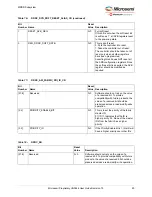
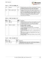
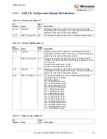
3.11.4
PHY Configuration Register Summary
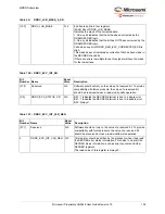
3.11.5
PHY Configuration Register Bit Definitions
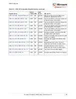
3.11.6
DDR_FIC Configuration Registers Summary
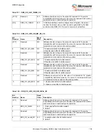
Table 102 •
PHY Configuration Register Summary
Register Name
Offset
Type
Reset
Source
Description
Reserved
0×200 to 0×22C
-
-
-
0×230
RW
PRESET_N PHY data slice in use register
Reserved
0×234 to 0×3C8
-
-
-
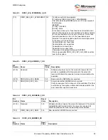
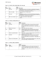
Table 103 •
PHY_DATA_SLICE_IN_USE_CR
Bit
Number
Name
Reset
Value
Description
[31:5]
Reserved
0×0
Software should not rely on the value of a reserved bit.
To provide compatibility with future products, the value
of a reserved bit should be preserved across a read-
modify-write operation.
[4:0]
REG_PHY_DATA_SLICE_IN_USE
0×0
Data bus width selection for read FIFO RE generation.
One bit for each data slice.
1: Data slice is valid.
0: Read data responses are ignored.
Note:
The PHY data slice 0 must always be
enabled.
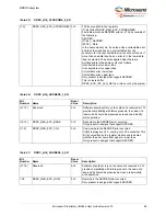
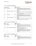
Table 104 •
DDR_FIC Configuration Register Summary
Register Name
Addres
s Offset R/W
Reset
Source
Description
0×400
RW
PRESET_
N
Indicates the base address of the non-
bufferable address region.
0×404
RW
PRESET_
N
Indicates the size of the non-bufferable
address region.
0×408
RW
PRESET_
N
10-bit timer interface used to configure the
timeout register.
0×40C
RW
PRESET_
N
Enable write buffer and read buffer register
for AHBL master1 and master2.
0×410
RW
PRESET_
N
Invalidates write buffer and read buffer for
AHBL master1 and master2.
0×414
RW
PRESET_
N
Clear bit for error status by AHBL master1
and master2 write buffer.
0×418
RW
PRESET_
N
Used for Interrupt generation.


