MDDR Subsystem
Microsemi Proprietary UG0446 User Guide Revision 7.0
73
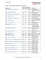
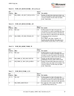
[3:0]
REG_DDRC_ADDRMAP_ROW_B15 0×0
Selects the address bit used as row address bit 15.
Valid range: 0 to 11, and 15
Internal base: 21
The selected address bit is determined by adding the
internal base to the value of this field.
If set to 15, row address bit 15 is set to 0.
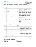
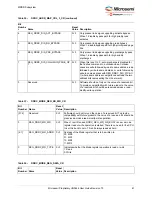
Table 39 •
DDRC_INIT_1_CR
Bit
Number
Name
Reset
Value
Description
[31:12]
Reserved
0×0
Software should not rely on the value of a reserved bit. To
provide compatibility with future products, the value of a
reserved bit should be preserved across a a read-modify-
write operation.
[11:8]
REG_DDRC_PRE_OCD_X32
0×0
Wait period before driving the on chip driver calibration
(OCD) Complete command to DRAM.
Units are in counts of a global timer that pulses every 32
clock cycles.
There is no known specific requirement for this. It may be
set to zero.
[7:1]
REG_DDRC_FINAL_WAIT_X32
0×0
Cycles to wait after completing the DRAM initialization
sequence before starting the dynamic scheduler.
Units are in counts of a global timer that pulses every 32
clock cycles.
There is known specific requirement for this; it may be set to
zero.
0
REG_DDRC_SKIP_OCD
0×1
This register must be kept at 1.
1: Indicates the controller is to skip the on chip driver
calibration (OCD) adjustment step during DDR2
initialization. OCD_Default and OCD_Exit are performed
instead.
0: Not supported
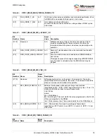
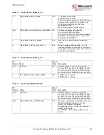
Table 40 •
DDRC_CKE_RSTN_CYCLES_1_CR
Bit
Number Name
Reset
Value
Description
[31:16]
Reserved
0×0
Software should not rely on the value of a reserved bit. To
provide compatibility with future products, the value of a
reserved bit should be preserved across a read-modify-write
operation.
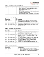
Table 38 •
DDRC_ADDR_MAP_ROW_2_CR

