Fabric DDR Subsystem
Microsemi ProprietaryUG0446 User Guide Revision 7.0
147
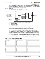
base clock (FDDR_SUBSYSTEM_CLK) for the FDDR comes from a fabric CCC or an external source
through the FPGA fabric. The FDDR clock controller is associated with a dedicated PLL (FPLL) for clock
synthesis and de-skewing the internal DDR_FIC clock from the base clock.
The FDDR clock controller consists of an FPLL and fabric alignment clock controller (FACC).
4.6.3.1.1
FPLL
The FDDR_SUBSYSTEM_CLK from the FPGA fabric is used as a reference clock to the FPLL, and is
multiplied to generate a clock frequency of up to 333 MHz. The FDDR_SUBSYSTEM_CLK can be
generated from a fabric CCC/PLL, one of the on-chip oscillators, or directly from multi-standard user I/Os
(MSIO) through FPGA fabric.
The supplies required to power the FPLL are the device core supply (VDD) for the digital section and the
analog supply (FDDR_PLL_VDDA) for analog section. The required voltage for the FDDR_PLL_VDDA is
2.5 V or 3.3 V, based on the power supply availability on the board. The analog power supply voltage (2.5
V or 3.3 V) does not impact the FPLL frequency range. Refer to the DS0128: IGLOO2 and SmartFusion2
Datasheet or the FPLL operational range and characteristics.
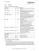
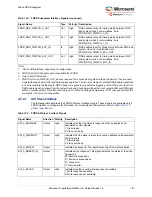
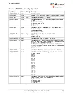
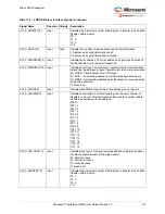
The FPLL generates a lock signal (FPLL_LOCK) to indicate that the FPLL is locked onto the
FDDR_SUBSYSTEM_CLK signal. The precision of the FPLL_LOCK discrimination can be adjusted
using the lock window controls. The lock window represents the phase error window for lock assertion.
The lock window can be adjusted between 500 parts per million (ppm) and 32,000 ppm in powers of 2.
The integration of the lock period can be adjusted using a built-in lock counter. The lock counter or lock
delay indicates the number of reference clock cycles to wait after the FPLL is locked for asserting the
FPLL_LOCK signal. The lock delay is useful for avoiding false toggling of the FPLL lock signal. The lock
counter can be configured between 32 and 32,768 cycles in multiples of 2.
There are two interrupts to indicate FPLL lock assertion and deassertion.
4.6.3.1.2
FACC
Within the FDDR clock controller, the FACC is responsible for interfacing with the FPLL, generating the
aligned clocks required by the FDDR subsystem, and controlling the alignment of FPGA fabric interface
clocks.
The clocks generated by the FACC are as follows:
•
FDDR_CLK clocks the FDDR subsystem. FDDR_CLK can be operated up to 333 MHz, depending
on the type of DDR present in the system.
•
FDDR_SUBSYSTEM_CLK clocks the DDR_FIC, and defines the frequency at which the connected
FPGA fabric subsystem is intended to operate.
•
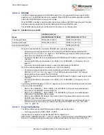
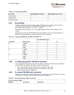
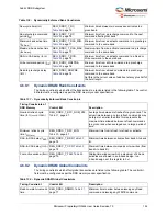
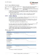
The possible FDDR_CLK:DDR_ FIC_CLK ratios are 1:1, 2:1, 3:1, 4:1, 6:1, 8:1, 12:1, and 16:1.
The FACC includes no-glitch multiplexers (NGMUXs) to feed the DDR_FIC clock with a standby clock
(CK_STANDBY) during the FPLL initialization. During initialization, the FDDR is not operational until after
FPLL lock is achieved. However, the glitch-free multiplexers are still used to ensure that the clock being
driven to DDR_FIC during this time comes from the RC oscillator, avoiding the potentially high frequency
output of the FPLL, which may be outside of the supported range of operation of DDR_FIC.
4.6.3.1.3
FPLL Initialization
In order to attain clock alignment between the FPGA fabric and the FDDR subsystem, it is necessary to
use the FPLL to perform de-skewing of the FDDR clocks. After the FPLL is initialized, it typically takes
over 500 divided reference clock cycles for lock to be achieved. The FPLL lock assertion time is also
dependent on the FPLL lock parameters (lock window and lock delay). There is no provision made for
operation of the FDDR subsystem before FPLL lock is achieved.
4.6.3.1.4
PLL Lock Monitoring
The FDDR has an input, CLK_BASE_PLL_LOCK, to monitor the fabric PLL lock. It must be connected to
the lock signal generated by the fabric PLL which is being used to generate the base clock to the FDDR.
Within the FDDR subsystem, there are two interrupts related to the PLL lock. A lock interrupt, indicating
FPLL lock achieved, and an FPLL lock lost interrupt. Each of these two interrupts has a corresponding
interrupt enable bit in the FDDR subsystem registers. It is also possible to read the state of the two PLL
lock signals through the FDDR registers.


