MDDR Subsystem
Microsemi Proprietary UG0446 User Guide Revision 7.0
30
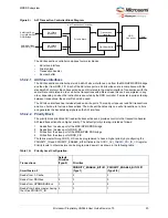
The DDR controller has a transaction store, shared for low and high priority transactions. The
register can be configured for allocating the transaction store between the
low and high priority transactions. For example, if the
field is
configured to 0, the controller allocates more time to high priority transactions. The ratio for LPR: HPR is
1:7 (as the transaction store depth is 8).
The
registers can be configured for the minimum clock values for treating
the transactions in the HPR, LPR, and WR queue as critical and non-critical.
To force all incoming transactions to low priority, configure the
default it is configured to force all the incoming transactions to low priority.
3.5.5.11 Refresh Controls
The DDR controller automatically issues refresh commands to DDR memory for every tRFC (min). The
DDR controller can be programmed to issue single refreshes at a time
(REG_DDRC_REFRESH_BURST = 0) to minimize the worst-case impact of a forced refresh cycle. It
can be programmed to burst the maximum number of refreshes allowed for DDR (REFRESH_BURST =
7, for performing 8 refreshes at a time) to minimize the bandwidth lost when refreshing the pages.
3.5.5.12 1T or 2T Timing
The DRAM can be used in 1T or 2T Timing mode by configuring the
register. The address bus can be clocked using 1T or 2T clocking. With 1T, the DDR controller can issue
a new command on every clock cycle. In 2T timing, the DDR controller holds the address and command
bus valid for two clock cycles. This reduces the efficiency of the bus to one command per two clocks, but
it doubles the amount of setup and hold time. The data bus remains the same for all of the variations in
the address bus and the default configuration is 1T timing mode.
3.5.5.13 ODT Controls
The ODT for a specific rank of memory can be enabled or disabled by configuring the
registers. These must be configured
before taking the controller out of soft reset. They are applied to every read or write issued by the
controller.
3.5.5.14 Soft Resets
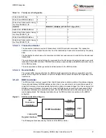
Set the REG_DDRC_SOFT_RSTB bit of
to 0 to reset the DDR
controller. To release the DDR controller from reset, set the REG_DDRC_SOFT_RSTB bit of
to 1.
3.5.5.15 MDDR Memory Map
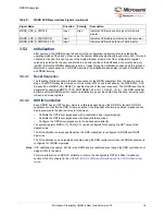
The address map to access the DDR memory from MSS/HPMS masters through MDDR is 0xA0000000-
0xDFFFFFFF, which is 1 GB. But the MDDR can support up to 4 GB of memory, out of which only 1 GB
of this memory is accessible at a time from the MSS/HPMS masters through the AHB bus matrix.
DDR_FIC can access the entire 4 GB memory.
To enable MSS/HPMS masters to access 4 GB, the DDR address space (0x00000000-0xFFFFFFFF) is
divided into 16 DDR regions, as shown in
. Each region is 256 MB (4 regions
together form 1 GB). The HPMS masters can access any of these four regions at a time, depending on
the Address Space Mapping mode configured for that particular master using the
register in
SYSREG. For SmartFusion2, the DDRB_CR register has four 4-bit fields
(DDR_IDC_MAP,DDR_SW_MAP, DDR_HPD_MAP, and DDR_DS_MAP). For Igloo2, the
register has two 4-bit fields (DDR_SW_MAP, DDR_HPD_MAP) whose bits can be configured to select
the DDR Address Space Mapping modes from 0 to 12.
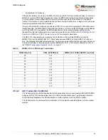
The Address Space Mapping modes for a 4 GB memory are shown in
. For example,
if the DDR_SW_MAP is configured as 0001, then the AHB bus matrix can access 0, 1, 2, and 3 regions

