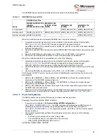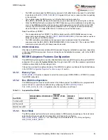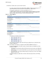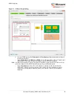
MDDR Subsystem
Microsemi Proprietary UG0446 User Guide Revision 7.0
22
3.5.4.3.1
Address Mapping
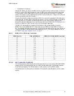
Read and write requests to the DDR controller requires a system address. The controller is responsible
for mapping this system address with rank, bank, row, and column address to DRAM.
The address mapper maps linear request addresses to DDR memory addresses by selecting the source
bit that maps to each and every applicable DDR memory address bit. The address map interface
registers can be configured to map source address bits to DRAM address (for more information, refer to
"Address Mapping" section on page 27
in Configuring the MDDR features).
3.5.4.3.2
Transaction Scheduling
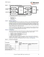
The DDR controller schedules the read and write transactions to DDR memory. The DDR controller
classifies the transactions into three types, based on the commands from the AXI transaction controller:
•
Low priority reads (LPR)
•
High priority reads (HPR)
•
Writes (WR)
Each type of transaction has a queue and the queued transactions can be in normal state or in critical
state. The transactions in a queue moves from normal state to critical state when that transaction is not
serviced for a count of MAX_STARVE_X32 clocks. The MAX_STARVE_X32 values for each queue can
be configured using the DDR controller performance registers (refer
"Performance" section on page 29
).
The DDR controller completes the critical transactions with high priority.
3.5.4.3.3
Write Combine
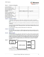
The DDR controller combines multiple writes to the same address into a single write to DDR memory.
When a new write collides with the queued write, the DDR controller overwrites the data for the queued
write with that from the new write and only performs one write transaction. The write combine
functionality can be disabled by setting the register bit
to 1.
3.5.4.3.4
SECDED
The DDR controller supports built-in SECDED capability for correcting single-bit errors and detecting
two-bit errors. The SECDED feature can be enabled in the
System Builder - memory controller
configuration
window. When SECDED is enabled, the DDR controller adds 8 bits of SECDED data to
every 64 bits of data.
The DDR controller computes ECC for every 64-bit data. When SECDED is enabled, a write operation
computes and stores a SECDED code along with the data, and a read operation reads and checks the
data against the stored SECDED code. It is therefore, possible to receive single/dual bit errors when
reading uninitialized memory locations. To avoid this, all the memory locations must be written before
being read.
For a non 64-bit write operation, the DDR controller performs a 256-bit read modify write (RMW)
operation. This read modify write operation is always performed on 256-bit aligned addresses.
For example, if the DDR controller receives a 32-bit write operation to address 0x4, then the DDR
controller performs the following operations:
1.
Reads the 256-bit data from 0x0(256-bit aligned address for 0x4).
2.
Modifies 32-bits (bit33 to bit64) of that 256-bit data with the user 32-bit data.
3.
Computes the ECC and writes 288-bits (256-bit data + 32-bit ECC) to address 0x0.
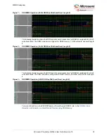
The following illustration shows the DDR controller burst transactions to DRAM for unaligned 64-bit AXI
write transaction. The DDR controller is configured for DDR3 memory, 32-bit burst width, and burst
length 8.

