MDDR Subsystem
Microsemi Proprietary UG0446 User Guide Revision 7.0
27
3.5.5.5.1
Dynamic DRAM Rank Constraints
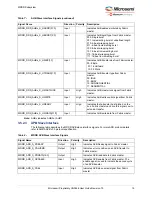
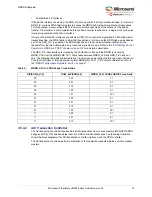
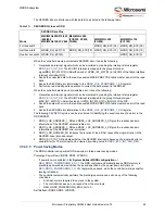
The timing constraints that affect the transactions to a rank are listed in the following table. The control bit
field must be configured as per the DDR memory vendor specification.
3.5.5.5.2
Dynamic DRAM Global Constraints
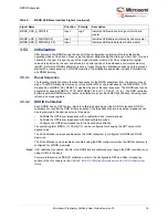
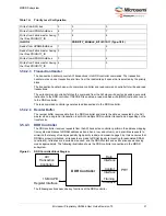
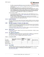
The timing constraints that affect global transactions are listed in the following table. The control bit field
must be configured as per the DDR memory vendor specification.
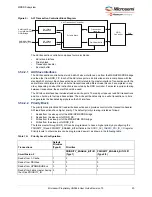
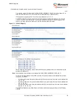
The DDR memories require delays after initializing the mode registers. The following registers must be
configured for the delay requirements for the DDR memories. The DDR controller uses these delay
values while initializing the DDR memories.
•
(recommended value is 0x4242)
•
(recommended value is 0x8)
3.5.5.6
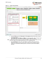
Address Mapping
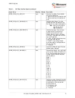
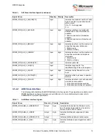
The DDR controller maps linear request addresses to DDR memory addresses by selecting the source
bit that maps to each and every applicable DDR memory address bit.
Each DDR memory address bit has an associated register vector to determine its source. The source
address bit number is determined by adding the internal base of a given register to the programmed
value for that register, as described in
.
Table 15 •
Dynamically-Enforced Bank Constraints
Timing Constraints of DDR
Memory
Control Bit
Description
Nominal refresh cycle time
(t
RFC(nom
) or t
REFI
)
Average time between refreshes for a given rank.
The actual time between any two refresh
commands may be larger or smaller than this; this
represents the maximum time allowed between
refresh commands to a given rank when averaged
over a large period of time.
Minimum refresh cycle time
t
RFC(min)
Minimum time from refresh to refresh or activate.
RAS-to-rAS delay (t
RRD
)
Minimum time between activates from bank A to
bank B.
RAS-to-CAS delay (t
CCD
)
Minimum time between two reads or two writes
(from bank A to bank B).
Four active window (t
FAW
)
Sliding time window in which a maximum of:
4 bank activates are allowed in an 8-bank design.
In a 4-bank design, set this register to 0x1.
Table 16 •
Dynamic DRAM Global Constraints
Timing Constraint
Control Bit
Description
Read-to-write turnaround time
(t
RTW
)
Minimum time to allow between issuing any
Read command and issuing any WRITE
command
Write-to-read turnaround time
(t
RTR
)
Minimum time to allow between issuing any Write
command and issuing any Read command
Write latency
Time after a Write command that write data
should be driven to DRAM.

