MDDR Subsystem
Microsemi Proprietary UG0446 User Guide Revision 7.0
10
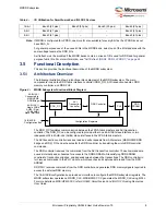
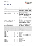
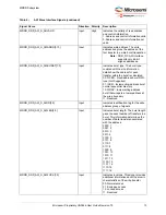
Note:
1
AXI or AHB interface, depending on configuration.
2
MDDR_DQS_N[3:0] signals are not available for LPDDR.
3
TMATCH_IN and TMATCH_OUT pins are required to be connected together outside the device. They
are used for gate training as part of the read data capture operation. The two pins create an internal DQS
Enable signal that is used to calibrate the flight path. DQS needs to be gated to prevent false triggering of
the FIFO write clock. This DQS Enable signal is derived from the system clock and physically matches
the clock output buffer and DQS input buffer to compensate for I/O buffer uncertainty due to Process-
Voltage-Temperature (PVT) changes. Without this connection, the circuit is not operable.
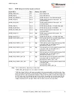
MDDR_ADDR[15:0]
Out
–
Dram address bits
MDDR_BA[2:0]
Out
–
Dram bank address
MDDR_DM_RDQS[3:0]
In/out
–
DRAM data mask – from bidirectional pads
MDDR_DQS[3:0]
In/out
–
DRAM single-ended data strobe output – for
bidirectional pads
MDDR_DQS_N[3:0]
In/out
–
DRAM single-ended data strobe output – for
bidirectional pads
MDDR_DQ[31:0]
In/out
–
DRAM data input/output – for bidirectional pads
MDDR_DQ_ECC[3:0]
In/out
–
DRAM data input/output for SECDED
MDDR_DM_RDQS_ECC
In/out
High
DRAM single-ended data strobe output – for
bidirectional pads
MDDR_DQS_ECC
In/out
High
DRAM single-ended data strobe output – for
bidirectional pads
MDDR_DQS_ECC_N
In/out
Low
DRAM data input/output – for bidirectional pads
MDDR_DQS_TMATCH_0_IN
In
High
DQS enables input for timing match between DQS
and system clock. For simulations, tie to
MDDR_DQS_TMATCH_0_OUT.
MDDR_DQS_TMATCH_1_IN
In
High
DQS enables input for timing match between DQS
and system clock. For simulations, tie to
MDDR_DQS_TMATCH_1_OUT.
MDDR_DQS_TMATCH_0_OUT
Out
High
DQS enables output for timing match between DQS
and system clock. For simulations, tie to
MDDR_DQS_TMATCH_0_IN.
MDDR_DQS_TMATCH_1_OUT
Out
High
DQS enables output for timing match between DQS
and system clock. For simulations, tie to
MDDR_DQS_TMATCH_1_IN.
MDDR_DQS_TMATCH_ECC_IN
In
High
DQS enables input for timing match between DQS
and system clock. For simulations, tie to
MDDR_DQS_TMATCH_ECC_OUT.
MDDR_DQS_TMATCH_ECC_OUT
Out
High
DQS enables output for timing match between DQS
and system clock.
For simulations, tie to
MDDR_DQS_TMATCH_ECC_IN.
Table 5 •
MDDR Subsystem Interface Signals
(continued)
Signal Name
Type
Polarity
Description

