MDDR Subsystem
Microsemi Proprietary UG0446 User Guide Revision 7.0
74
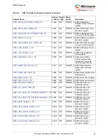
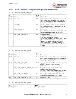
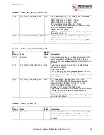
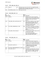
[15:8]
REG_DDRC_PRE_CKE_X1024
0×0
The 10-bit REG_DDRC_PRE_CKE_X1024 [9:0] value is
spit across the two registers:
DDRC_CKE_RSTN_CYCLES_1_CR and
DDRC_CKE_RSTN_CYCLES_2_CR.
[7:0] bits of REG_DDRC_PRE_CKE_X1024.
Cycles to wait after reset before driving CKE High to start
the DRAM initialization sequence.
Units: 1,024 clock cycles.
DDR2 specifications typically require this to be programmed
for a delay of
≥
200 µs.
[7:0]
REG_DDRC_DRAM_RSTN_X1024 0×0
Number of cycles to assert DRAM reset signal during
initialization sequence.
This is only present for implementations supporting DDR3
devices.
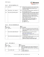
Table 41 •
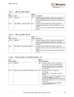
DDRC_ CKE_RSTN_CYCLES_2_CR
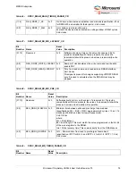
Bit
Number Name
Reset
Value
Description
[31:16]
Reserved
0×0
Software should not rely on the value of a reserved bit. To
provide compatibility with future products, the value of a
reserved bit should be preserved across a read-modify-write
operation.
[11:2]
REG_DDRC_POST_CKE_X1024
0×0
Cycles to wait after driving CKE High to start the DRAM
initialization sequence.
Units: 1,024 clocks.
DDR: Typically requires a 400 ns delay, requiring this value
to be programmed to 2 at all clock speeds.
SDR: Typically requires this to be programmed for a delay of
100 µs to 200 µs.
[1:0]
REG_DDRC_PRE_CKE_X1024
0×0
This field represents the upper 2 bits of the 10-bit
REG_DDRC_PRE_CKE_X1024 value split across the 2
registers DDRC_CKE_RSTN_CYCLES_1_CR and
DDRC_CKE_RSTN_CYCLES_2_CR.
[9:8] bits of REG_DDRC_PRE_CKE_X1024.
Cycles to wait from the start of reset assertion before driving
CKE High to start the DRAM initialization sequence.
Units: 1,024 clock cycles.
DDR2 specifications typically require this to be programmed
for a delay of
≥
200 µs.
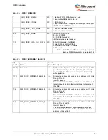
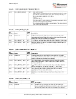
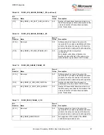
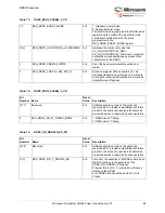
Table 42 •
DDRC_INIT_MR_CR
Bit
Number
Name
Reset
Value
Description
[31:16]
Reserved
0×0
Software should not rely on the value of a reserved bit. To
provide compatibility with future products, the value of a
reserved bit should be preserved across a read-modify-write
operation.
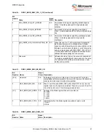
Table 40 •
DDRC_CKE_RSTN_CYCLES_1_CR

