MDDR Subsystem
Microsemi Proprietary UG0446 User Guide Revision 7.0
82
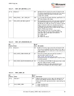
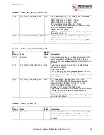
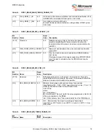
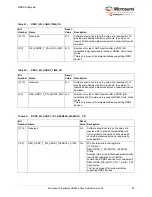
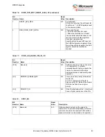
[31:16]
Reserved
0×0
Software should not rely on the value of a reserved bit. To provide
compatibility with future products, the value of a reserved bit should be
preserved across a read-modify-write operation.
[15:0]
REG_DDRC_MR_DATA
0×0
Mode register write data
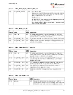
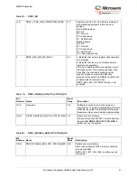
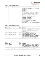
Table 59 •
DDRC_PWR_SAVE_1_CR
Bit
Number Name
Reset
Value Description
[31:13]
Reserved
0×0
Software should not rely on the value of a
reserved bit. To provide compatibility with future
products, the value of a reserved bit should be
preserved across a read-modify-write
operation.
[12:6]
REG_DDRC_POST_SELFREF_GAP_X32
0×10
Minimum time to wait after coming out of self
refresh before doing anything. This must be
larger than all the constraints that exist
(Specifications: maximum of t
XSNR
and t
XSRD
and t
XSDLL
, which is 512 clocks).
Unit: Multiples of 32 clocks.
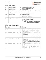
[5:1]
REG_DDRC_POWERDOWN_TO_X32
0×06
After this many clocks of NOP or DESELECT,
the controller puts the DRAM into power-down.
This must be enabled in the Master Control
register.
Unit: Multiples of 32 clocks.
0
REG_DDRC_CLOCK_STOP_EN
0×0
1: Stops the clock to the PHY whenever a clock
is not required by LPDDR1.
0: Clock will never be stopped.
This is only present for implementations
supporting mobile/LPDDR1 devices.
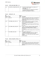
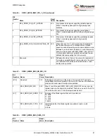
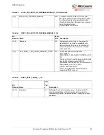
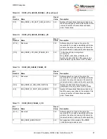
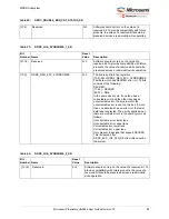
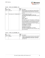
Table 60 •
DDRC_PWR_SAVE_2_CR
Bit
Number Name
Reset
Value Description
[31:12]
Reserved
0×0
Software should not rely on the value of a
reserved bit. To provide compatibility with future
products, the value of a reserved bit should be
preserved across a read-modify-write operation.
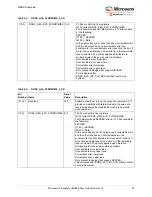
11
REG_DDRC_DIS_PAD_PD
0×0
1: Disable the pad power-down feature.
0: Enable the pad power-down feature.
Used only in non-DFI designs.
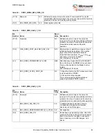
[10:3]
REG_DDRC_DEEPPOWERDOWN_TO_X1024 0×0
Not supported.
[2:0]
REG_DDRC_PAD_PD
0×0
If pads have a power-saving mode, this is the
greater of the time for the pads to enter power-
down or the time for the pads to exit power-
down. Used only in non-DFI designs. Unit:
clocks.
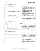
Table 58 •
DDRC_MODE_REG_DATA_CR

