MDDR Subsystem
Microsemi Proprietary UG0446 User Guide Revision 7.0
28
[Internal base] + [register value] = [source address bit number]
EQ 1
For example, reading the description for REG_DDRC_ADDRMAP_COLB3, the internal base is 3; so
when the full data bus is in use, the column bit 4 is determined by 3+ [register value].
If this register is programmed to 2, then the source address bit is: 3+2 = 5.
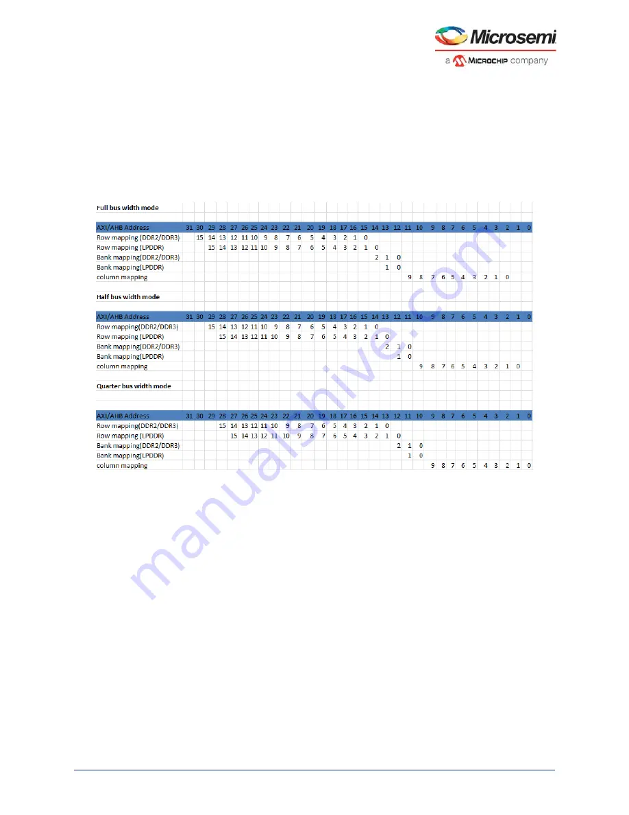
The DDR configurator assigns values to the address mapping registers depending on the selected
number of columns, rows and banks. The following illustration provides the default mapping of the
memory row, bank, and column address to the user interface address domain.
Figure 10 •
Address Mapping
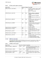
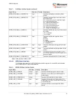
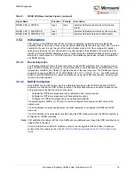
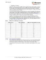
The following are the address mapping registers:
•
•
•
•
•
•
While configuring the registers, ensure that two DDR memory address bits are not determined by the
same source address bit.
Note:
Some registers map multiple source address bits (REG_DDRC_ADDRMAP_ROW_B0_11).
To arrive at the right address for the DDR controller, the system address or AXI address bits [4:0] are
mapped by the MDDR.
•
In full bus width mode, the system address bits [4:0] are used to map the lower column address bits
(C0, C1, C2).
•
In half bus width mode, the system address bits [4:0] are used to map the lower column address bits
(C0, C1, C2, C3).
•
In quarter bus width mode, the system address bits [4:0] are used to map the lower column address
bits (C0, C1, C2, C3, C4).
The MDDR configurator uses (Row, Bank, and Column) address mapping as shown in the following
example.

