MDDR Subsystem
Microsemi Proprietary UG0446 User Guide Revision 7.0
9
3.5.2
Port List
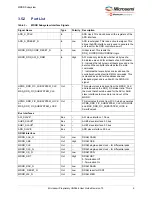
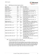
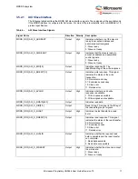
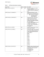
Table 5 •
MDDR Subsystem Interface Signals
Signal Name
Type
Polarity
Description
APB_S_PCLK
In
–
APB clock. This clock drives all the registers of the
APB interface.
APB_S_PRESET_N
In
Low
APB reset signal. This is an active low signal. This
drives the APB interface and is used to generate the
soft reset for the DDR controller as well.
MDDR_DDR_CORE_RESET_N
In
Low
Global reset. This resets the
DDR_FIC/DDRC/PHY/DDRAXI logic.
MDDR_DDR_AXI_S_RMW
In
High
AXI mode only Indicates whether all bytes of a
64-bit lane are valid for all beats of an AXI transfer.
0: Indicates that all bytes in all beats are valid in the
burst and the controller should default to write
commands.
1: Indicates that some bytes are invalid and the
controller should default to RMW commands. This
is classed as an AXI write address channel
sideband signal and is valid with the AWVALID
signal.
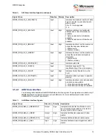
HPMS_DDR_FIC_SUBSYSTEM_CLK
or,
MSS_DDR_FIC_SUBSYSTEM_CLK
Out
–
This output clock is derived from the MDDR_CLK
and is based on the DDR_FIC divider ratio. This is
the clock that should be used for the AXI or AHB
slave interfaces to move data in and out of the
MDDR.
HPMS_DDR_FIC_SUBSYSTEM_LOCK
or,
MSS_DDR_FIC_SUBSYSTEM_LOCK
Out
–
This indicates the lock from FCCC which generates
HPMS_DDR_FIC_SUBSYSTEM_CLK for IGLOO2
and MSS_DDR_FIC_SUBSYSTEM_LOCK in
SmartFusion2.
Bus Interfaces
AXI_SLAVE
1
Bus
–
AXI slave interface 1.0 bus
AHB0_SLAVE
2
Bus
–
AHB0 slave interface 3.0 bus
AHB1_SLAVE
3
Bus
–
AHB1 slave interface 3.0 bus
APB_SLAVE
Bus
–
APB slave interface 3.0 bus
DRAM Interface
MDDR_CAS_N
Out
Low
DRAM CASN
MDDR_CKE
Out
High
DRAM CKE
MDDR_CLK
Out
–
DRAM single-ended clock – for differential pads
MDDR_CLK_N
Out
–
DRAM single-ended clock – for differential pads
MDDR_CS_N
Out
Low
DRAM CSN
MDDR_ODT
Out
High
DRAM ODT.
0: Termination Off
1: Termination On
MDDR_RAS_N
Out
Low
DRAM RASN
MDDR_ RESET_N
Out
Low
DRAM reset for DDR3
MDDR_WE_N
Out
Low
DRAM WEN


