MDDR Subsystem
Microsemi Proprietary UG0446 User Guide Revision 7.0
78
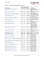
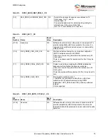
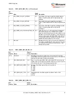
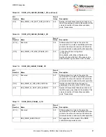
[4:0]
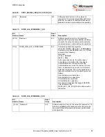
REG_DDRC_WR2RD
0×0
WL + tWTR + BL/2
Minimum time from WRITE command to READ command. Includes
time for bus turnaround and recovery times and all per-bank, per-
rank, and global constraints. Unit: clocks.
where,
WL: Write latency.
BL: Burst length. This should match the value programmed in the BL
bit of the mode register to the DRAM.
t
WTR
: Internal WRITE to READ command delay. This comes directly
from the DRAM specifications.
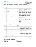
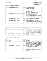
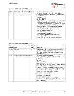
Table 52 •
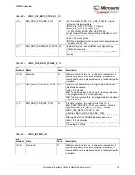
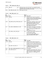
DDRC_DRAM_T_PD_CR
Bit
Number
Name
Reset
Value
Description
[31:9]
Reserved
0×0
Software should not rely on the value of a reserved bit. To provide
compatibility with future products, the value of a reserved bit should be
preserved across a read-modify-write operation.
[8:4]
REG_DDRC_T_XP
0×0
t
XP
: Minimum time after power-down exit to any operation. Units: clocks
[3:0]
REG_DDRC_T_CKE
0×0
Minimum number of cycles of CKE High/Low during power-down and
self refresh. Unit: clocks
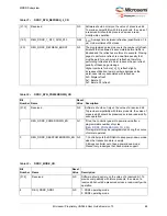
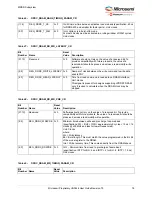
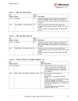
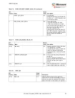
Table 53 •
DDRC_DRAM_BANK_ACT_TIMING_CR
Bit
Number
Name
Reset
Value
Description
[31:14]
Reserved
0×0
Software should not rely on the value of a reserved bit. To provide
compatibility with future products, the value of a reserved bit should be
preserved across a read-modify-write operation.
[13:10]
REG_DDRC_T_RCD
0×0
t
RCD
: Minimum time from activate to READ or WRITE command to
same bank (specification: 15 ns for DDR2-400 and lower for faster
devices). Unit: clocks.
[9:7]
REG_DDRC_T_CCD
0×0
t
CCD
: Minimum time between two reads or two writes (from bank A to
bank B) (specification: 2 cycles) is this value + 1. Unit: clocks.
[6:4]
REG_DDRC_T_RRD
0×0
t
RRD
: Minimum time between activates from bank A to bank B
(specification: 10 ns or less). Unit: clocks.
[3:0]
REG_DDRC_T_RP
0×0
t
RP
: Minimum time from precharge to activate of same bank. Unit:
clocks.
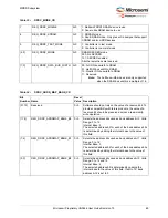
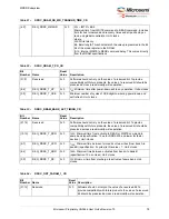
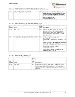
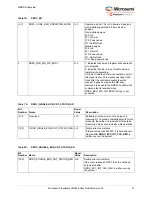
Table 54 •
DDRC_ODT_PARAM_1_CR
Bit
Number Name
Reset
Value Description
[31:12]
Reserved
0×0
Software should not rely on the value of a reserved bit. To
provide compatibility with future products, the value of a reserved
bit should be preserved across a read-modify-write operation.
Table 51 •
DDRC_DRAM_RD_WR_TRNARND_TIME_CR

