MDDR Subsystem
Microsemi Proprietary UG0446 User Guide Revision 7.0
69
7
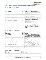
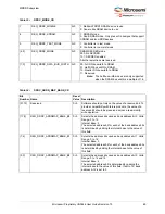
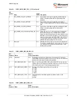
REG_DDRC_MOBILE
0×0
1: Mobile/LPDDR1 DRAM device in use
0: Non-mobile DRAM device in use
6
REG_DDRC_SDRAM
0×0
1: SDRAM mode
0: Non-SDRAM mode. Only present in designs that support
SDRAM and/or mSDR devices.
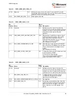
5
REG_DDRC_TEST_MODE
0×0
1: Controller is in test mode
0: Controller is in normal mode
[4:2]
REG_DDRC_MODE
0×0
DRAM SECDED mode
000: No SECDED
101: SECDED enabled
All other selections are reserved.
[1:0]
REG_DDRC_DATA_BUS_WIDTH 0×0
00: Full DQ bus width to DRAM
01: Half DQ bus width to DRAM
10: Quarter DQ bus width to DRAM
11: Reserved
Note:
The half bus width modes are only supported
when the DRAM bus width is a multiple of 16.
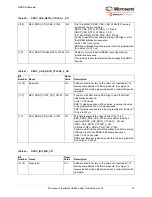
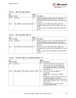
Table 34 •
DDRC_ADDR_MAP_BANK_CR
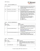
Bit
Number Name
Reset
Value Description
[31:12]
Reserved
0×0
Software should not rely on the value of a reserved bit. To
provide compatibility with future products, the value of a
reserved bit should be preserved across a read-modify-
write operation.
[11:8]
REG_DDRC_ADDRMAP_BANK_B0
0×0
Selects the address bits used as bank address bit 0. Valid
Range: 0 to 14
Internal Base: 2
The selected address bit for each of the bank address bits
is determined by adding the internal base to the value of
this field.
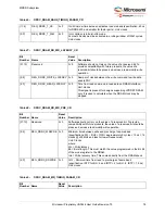
[7:4]
REG_DDRC_ADDRMAP_BANK_B1
0×0
Selects the address bits used as bank address bit 1. Valid
Range: 0 to 14
Internal Base: 3
The selected address bit for each of the bank address bits
is determined by adding the internal base to the value of
this field.
[3:0]
REG_DDRC_ADDRMAP_BANK_B2
0×0
Selects the address bits used as bank address bit 2. Valid
Range: 0 to 14 and 15
Internal Base: 4
The selected address bit is determined by adding the
internal base to the value of this field. If set to 15, bank
address bit 2 is set to 0.
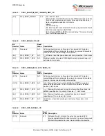
Table 33 •
DDRC_MODE_CR

