MDDR Subsystem
Microsemi Proprietary UG0446 User Guide Revision 7.0
112
3.12
Appendix A: How to Use the MDDR in SmartFusion2
This section describes how to use the MDDR subsystem in the design. It contains the following sections:
•
Design Flow Using System Builder
•
•
Use Model 1: Accessing MDDR from FPGA Fabric Through the AXI Interface
•
Use Model 2: Accessing MDDR from FPGA Fabric Through the AHB Interface
•
Use Model 3: Accessing MDDR from Cortex-M3 Processor
•
Use Model 4: Accessing MDDR from the HPDMA
3.12.1
Design Flow Using System Builder
This section describes how to use MDDR in the SmartFusion2 devices using the System Builder
graphical design wizard in the Libero Software.
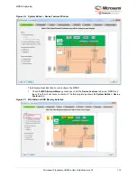
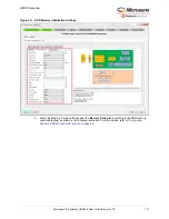
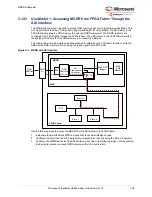
The following image shows the initial
System Builder
window where you can select the features that you
require. For details on how to launch and use the
System Builder
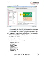
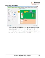
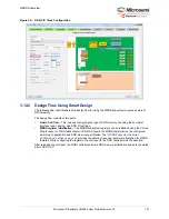
. For more information on DDR initialization, refer to the
Controller and Serial High Speed Controller Initialization Methodology
.
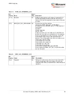
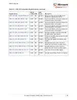
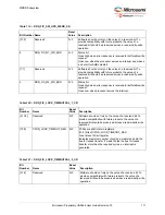
[3:0]
CFGR_LOCK_TIMEOUT_REG
0×0
20 bits are split into two registers.
[19:16] bits of CFGR_LOCK_TIMEOUT_REG
Lock timeout 20-bit register.
Indicates maximum number of cycles a master can hold the
bus for locked transfer. If master holds the bus for locked
transfer more than the required cycles, an interrupt is
generated.
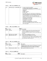
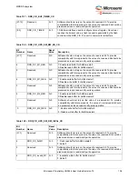
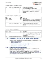
Table 122 •
DDR_FIC_LOCK_TIMEOUT_EN_CR
Bit
Number
Name
Reset
Value
Description
[31:1]
Reserved
0×0
Software should not rely on the value of a reserved bit. To
provide compatibility with future products, the value of a
reserved bit should be preserved across a read-modify-write
operation.
0
CFGR_LOCK_TIMEOUT_EN
0×0
1: Lock timeout feature is enabled and interrupt is
generated.
0: Lock timeout feature is disabled and interrupt is not
generated.
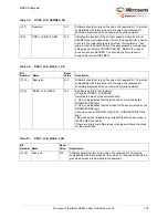
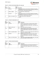
Table 123 •
DDR_FIC_RDWR_ERR_SR
Bit
Number
Name
Reset
Value
Description
[31:6]
Reserved
0×0
Software should not rely on the value of a reserved bit. To
provide compatibility with future products, the value of a
reserved bit should be preserved across a read-modify-
write operation.
[5:0]
DDR_FIC_CFG_RDWR_ERR_SR 0×0
Read address of math error register.
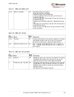
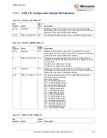
Table 121 •
DDR_FIC_LOCK_TIMEOUTVAL_2_CR

