ISD91200 Series Technical Reference Manual
Release Date: Sep 16, 2019
- 227 -
Revision 2.4
SPI0_MISO1, SPI0_MOSI0 and SPI0_MOSI1 will be set as data input ports.
SPI Controller
Master
SPICLKx
MISOx[1:0]
MOSIx[1:0]
SPISSx0
SPISSx1
Quad
SpiFlash
SCLK
MISO
MOSI
SS
MISOx[0]
MISOx[1]
MOSIx[0]
MOSIx[1]
WP
HOLDB
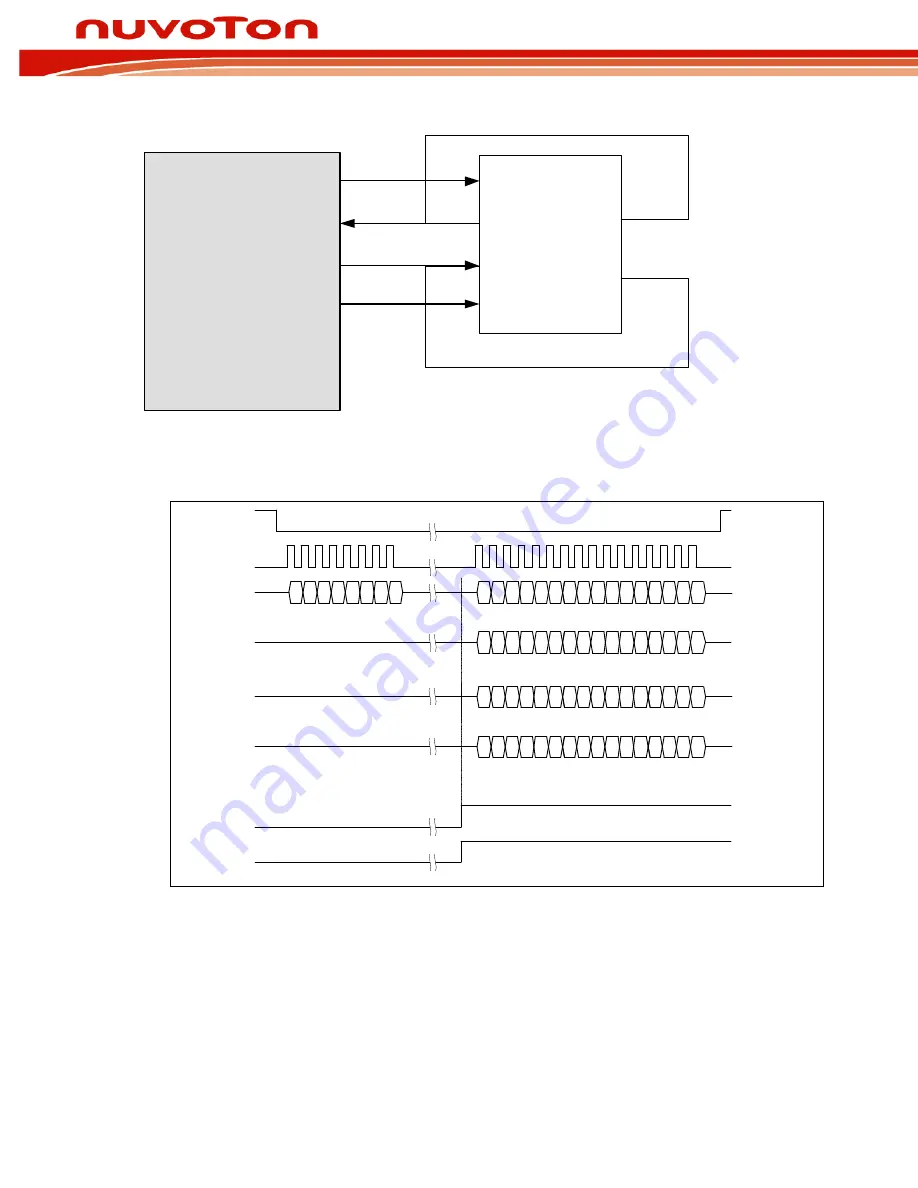
Figure 5-45 Quad Mode System Architecture
SPI_SS
7 6 5 4 3 2 1 0
SPI_CLK
SPI_MOSI0
SPI_MISO0
QUAD_IO_EN
4 0 4 0 4 0
5 1 5 1 5 1
QD_IO_DIR
Master output
Slave input
Master input
Slave output
Output
Output
SPI_MOSI1
SPI_MISO1
6 2 6 2 6 2
7 3 7 3 7 3
Output
Output
CS
CLK
DI (IO
0
)
DO (IO
1
)
WP (IO
2
)
HOLD (IO
3
)
4 0 4 0 4 0
5 1 5 1 5 1
6 2 6 2 6 2
7 3 7 3 7 3
4 0 4 0
5 1 5 1
6 2 6 2
7 3 7 3
Figure 5-46 Bit Sequence of Quad Output Mode
5.9.4.17
4-Level FIFO Buffer
The SPI controller is equipped with eight 32-bit wide transmit and receive FIFO buffers.
The transmit FIFO buffer is an 4-level depth, 32-bit wide, first-in, first-out register buffer. 4 words of
data can be written to the transmit FIFO buffer in advance through software by writing the SPI0_TX
register. The data stored in the transmit FIFO buffer will be read and sent out by the transmission
control logic. If the 8-level transmit FIFO buffer is full, the TXFULL bit will be set to 1. When the SPI


