R01UH0823EJ0100 Rev.1.00
Page 720 of 1823
Jul 31, 2019
RX23W Group
25. 16-Bit Timer Pulse Unit (TPUa)
25.9.10
Conflict between Buffer Register Write and Input Capture
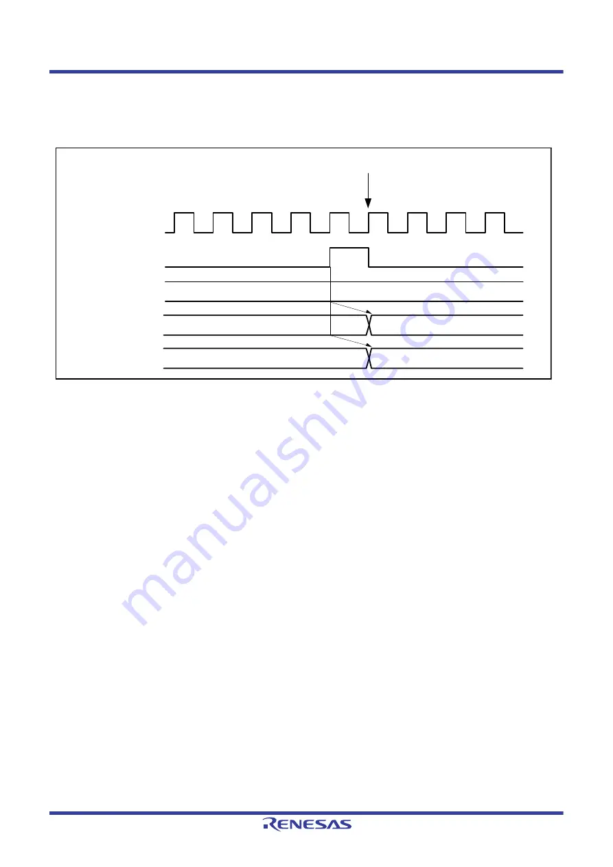
If the input capture signal is generated in a buffer register write cycle, the buffer operation takes precedence and the write
to the buffer register is not performed.
shows the timing in this case.
Figure 25.50
Conflict between Buffer Register Write and Input Capture
25.9.11
TCNT Simultaneous Input Capture in Cascade Operation
When TPU1.TCNT and TPU2.TCNT are cascaded for operation as a 32-bit counter, the counter value may not be
captured correctly even if the input capture signal is input to the TIOC1B and TIOC2B pins at the same time. This is
because a difference of up to 1 clock cycle in the timing of the capture signal to input to TPU1.TCNT and TPU2.TCNT
may occur due to internal delays.
For example, the counter value is captured at an overflow of TPU2.TCNT as in counting up from 0A31 FFFFh to
0A32 0000h, the value captured may be 0A31 0000h or 0A32 FFFFh.
The same applies to cascaded operation of TPU4.TCNT and TPU5.TCNT.
TCNT
TGRy
PCLK
Input capture signal
Buffer register
M
N
N
M
Buffer register write by CPU


