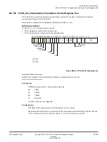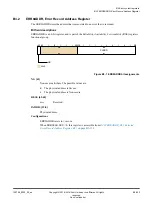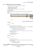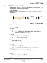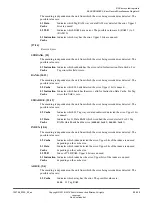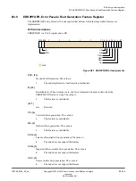
The encoding is dependent on the unit from which the error being recorded was detected. The
possible values are:
L1 Data
Cache
Indicates which Tag RAM way or data RAM way detected the error. Upper 2
bits are unused.
L2 TLB
Indicates which RAM has an error. The possible values are 0 (RAM 1) to 9
(RAM 10).
L1 Instruction
Cache
Indicates which way has the error. Upper 2 bits are unused.
[27:26]
Reserved,
RES0
.
SUBBANK, [25]
The encoding is dependent on the unit from which the error being recorded was detected. The
possible values are:
L1 Instruction
Cache
Indicates which subbank has the error, valid for Instruction Data Cache. For
Tag errors this field is zero.
BANK, [24:23]
The encoding is dependent on the unit from which the error being recorded was detected. The
possible values are:
L2 Cache
Indicates which L2 bank detected the error. Upper 1 bit is unused.
L1 Instruction
Cache
Indicates which bank has the error, valid for Instruction Data Cache. For Tag
errors this field is zero.
SUBARRAY, [22:19]
The encoding is dependent on the unit from which the error being recorded was detected. The
possible values are:
L2 Cache
Indicates which L2 Tag way or data doubleword detected the error. Upper 1 bit
is unused.
L1 Data
Cache
Indicates for L1 Data RAM which word had the error detected. For L1 Tag
RAMs which bank had the error (
0b0000
: bank0 ,
0b0001
: bank1)
INDEX, [18:6]
The encoding is dependent on the unit from which the error being recorded was detected. The
possible values are:
L2 Cache
Indicates which index detected the error. Upper bits of the index are unused
depending on the cache size.
L1 Data
Cache
Indicates which index detected the error. Upper bits of the index are unused
depending on the cache size.
L2 TLB
Index of TLB RAM. Upper 4 bits are unused.
L1 Instruction
Cache
Indicates which index has the error. Upper bits of the index are unused
depending on the cache size.
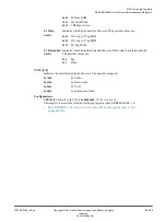
ARRAY, [5:4]
The encoding is dependent on the unit from which the error being recorded was detected. The
possible values are:
L2 Cache
Indicates which array has the error. The possible values are:
0b00
L2 Tag RAM.
B3 Error system registers
B3.5 ERR0MISC0, Error Record Miscellaneous Register 0
100798_0300_00_en
Copyright © 2016–2018 Arm Limited or its affiliates. All rights
reserved.
B3-299
Non-Confidential
Summary of Contents for Cortex-A76 Core
Page 4: ......
Page 22: ......
Page 23: ...Part A Functional description ...
Page 24: ......
Page 119: ...Part B Register descriptions ...
Page 120: ......
Page 363: ...Part C Debug descriptions ...
Page 364: ......
Page 401: ...Part D Debug registers ...
Page 402: ......
Page 589: ...Part E Appendices ...
Page 590: ......

