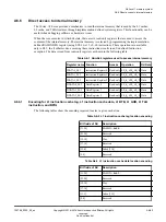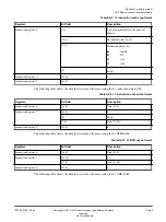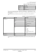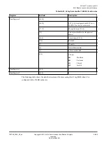
Table A6-16 L1 data TLB location encoding
Bit fields of Rd
Description
[31:24]
RAMID =
0x0A
[23:6]
Reserved
[5:0]
TLB Entry (0->47)
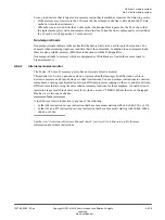
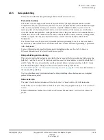
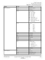
Data cache reads return 64 bits of data in Data Register 0, Data Register 1, and Data Register 2. If cache
protection is supported, Data Register 2 is used to report ECC information using the format shown in the
following tables.
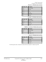
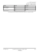
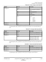
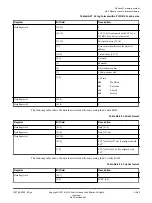
The following table shows the data that is returned from accessing the L1 data cache tag RAM with
ECC.
Table A6-17 L1 data cache tag format with ECC
Register
Bit field
Description
Data Register 0
[63:41]
0
[40:34]
ECC
[33]
Non-secure identifier for the physical
address
[32:5]
Physical address [39:12]
[4:3]
Reserved
[2]
Transient/WBNA
[1:0]
MESI
00
Invalid
01
Shared
10
Exclusive
11
Modified with respect to the L2
cache
Data Register 1
[63:0]
0
Data Register 2
[63:0]
0
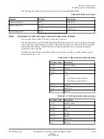
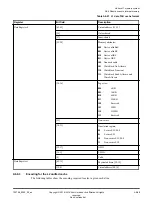
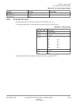
The following table shows the data that is returned from accessing the L1 data cache tag RAM without
ECC.
A6 Level 1 memory system
A6.6 Direct access to internal memory
100798_0300_00_en
Copyright © 2016–2018 Arm Limited or its affiliates. All rights
reserved.
A6-86
Non-Confidential
Summary of Contents for Cortex-A76 Core
Page 4: ......
Page 22: ......
Page 23: ...Part A Functional description ...
Page 24: ......
Page 119: ...Part B Register descriptions ...
Page 120: ......
Page 363: ...Part C Debug descriptions ...
Page 364: ......
Page 401: ...Part D Debug registers ...
Page 402: ......
Page 589: ...Part E Appendices ...
Page 590: ......


