D3.14
EDRCR, External Debug Reserve Control Register
The EDRCR is part of the Debug registers functional group.
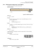
Bit field descriptions
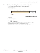
31 30 29 28 27 26 25 24 23 22 21 20 19 18 17 16 15 14 13 12 11 10 9 8 7 6 5 4 3 2 1 0
CSPA
CSE
RES
0
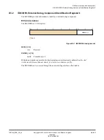
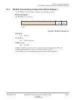
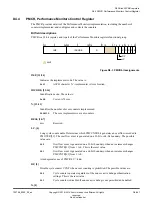
Figure D3-12 EDRCR bit assignments
RES0, [31:4]
RES0
Reserved.
CSPA, [3]
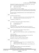
Clear Sticky Pipeline Advance. This bit is used to clear the EDSCR.PipeAdv bit to 0. The
actions on writing to this bit are:
0
No action.
1
Clear the EDSCR.PipeAdv bit to 0.
CSE, [2]
Clear Sticky Error. Used to clear the EDSCR cumulative error bits to 0. The actions on writing
to this bit are:
0
No action
1
Clear the EDSCR.{TXU, RXO, ERR} bits, and, if the core is in Debug state, the
EDSCR.ITO bit, to 0.
RES0, [1:0]
RES0
Reserved.
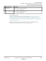
The EDRCR can be accessed through the internal memory-mapped interface and the external debug
interface, offset
0x090
.
Usage constraints
This register is accessible as follows:
Off
DLK OSLK SLK Default
Error Error Error
WI
WO
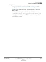
Configurations
EDRCR is in the Core power domain.
D3 Memory-mapped debug registers
D3.14 EDRCR, External Debug Reserve Control Register
100798_0300_00_en
Copyright © 2016–2018 Arm Limited or its affiliates. All rights
reserved.
D3-432
Non-Confidential
Summary of Contents for Cortex-A76 Core
Page 4: ......
Page 22: ......
Page 23: ...Part A Functional description ...
Page 24: ......
Page 119: ...Part B Register descriptions ...
Page 120: ......
Page 363: ...Part C Debug descriptions ...
Page 364: ......
Page 401: ...Part D Debug registers ...
Page 402: ......
Page 589: ...Part E Appendices ...
Page 590: ......

