5-22
MPC8240 Integrated Processor User’s Manual
Cache Implementation
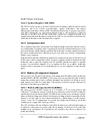
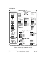
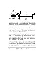
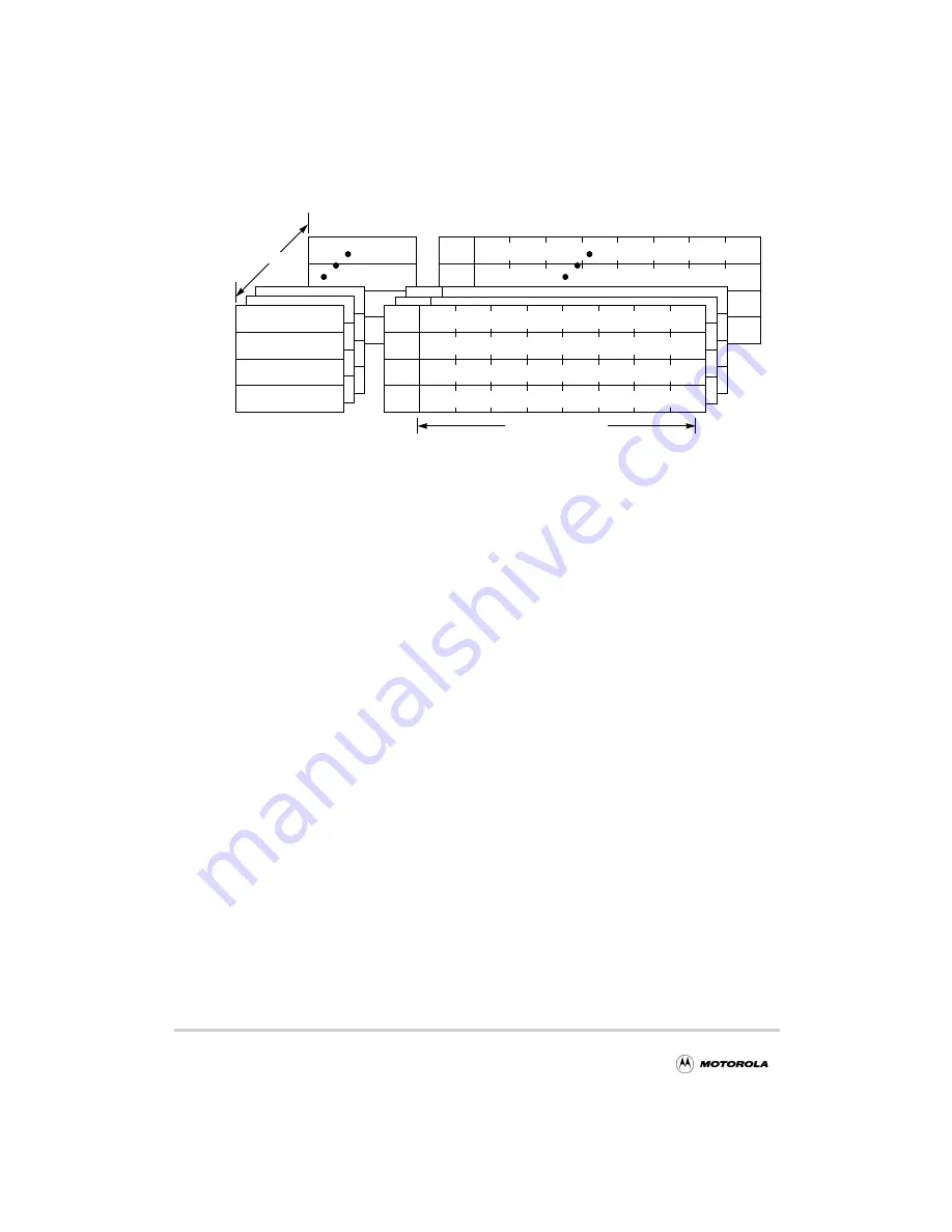
Figure 5-6. Data Cache Organization
Because the processor core data cache tags are single-ported, simultaneous load or store
and snoop accesses cause resource contention. Snoop accesses have the highest priority and
are given first access to the tags, unless the snoop access coincides with a tag write, in which
case the snoop is retried and must rearbitrate for access to the cache. Loads or stores that
are deferred due to snoop accesses are executed on the clock cycle following the snoop.
Because the caches on the processor core are write-back caches, the predominant type of
transaction to the memory subsystem for most applications is burst-read memory
operations, followed by burst-write memory operations, and single-beat (noncacheable or
write-through) memory read and write operations. When a cache block is filled with a burst
read, the critical double word is simultaneously written to the cache and forwarded to the
requesting unit, thus minimizing stalls due to load delays.
Additionally, there can be address-only operations, variants of the burst and single-beat
operations, (for example, global memory operations that are snooped and atomic memory
operations), and address retry activity (for example, when a snooped read access hits a
modified line in the cache). Note that all memory subsystem references are performed by
the processor core to the internal peripheral logic bus on the MC8240.
The address and data buses of the internal peripheral logic bus operate independently to
support pipelining and split transactions during memory accesses. The processor core
pipelines its own transactions to a depth of one level.
Typically, memory accesses are weakly ordered—sequences of operations, including
load/store string and multiple instructions, do not necessarily complete in the order they
begin—maximizing the efficiency of the internal bus without sacrificing coherency of the
data. The processor core allows pending read operations to precede previous store
operations (except when a dependency exists, or in cases where a non-cacheable access is
performed), and provides support for a write operation to proceed a previously queued read
data tenure (for example, allowing a snoop push to be enveloped by the address and data
Address Tag 1
Address Tag 2
Address Tag 3
Block 1
Block 2
Block 3
128 Sets
Address Tag 0
Block 0
8 Words/Block
State
State
State
Words 0–7
Words 0–7
Words 0–7
Words 0–7
State
Summary of Contents for MPC8240
Page 1: ...MPC8240UM D Rev 1 1 2001 MPC8240 Integrated Processor User s Manual ...
Page 38: ...xviii MPC8240 Integrated Processor User s Manual TABLES Table Number Title Page Number ...
Page 48: ...xlviii MPC8240 Integrated Processor User s Manual Acronyms and Abbreviations ...
Page 312: ...6 94 MPC8240 Integrated Processor User s Manual ROM Flash Interface Operation ...
Page 348: ...7 36 MPC8240 Integrated Processor User s Manual PCI Host and Agent Modes ...
Page 372: ...8 24 MPC8240 Integrated Processor User s Manual DMA Register Descriptions ...
Page 394: ...9 22 MPC8240 Integrated Processor User s Manual I2O Interface ...
Page 412: ...10 18 MPC8240 Integrated Processor User s Manual Programming Guidelines ...
Page 454: ...12 14 MPC8240 Integrated Processor User s Manual Internal Arbitration ...
Page 466: ...13 12 MPC8240 Integrated Processor User s Manual Exception Latencies ...
Page 516: ...16 14 Watchpoint Trigger Applications ...
Page 538: ...B 16 MPC8240 Integrated Processor User s Manual Setting the Endian Mode of Operation ...
Page 546: ...C 8 MPC8240 Integrated Processor User s Manual ...
Page 640: ...INDEX Index 16 MPC8240 Integrated Processor User s Manual ...

