6-90
MPC8240 Integrated Processor User’s Manual
ROM/Flash Interface Operation
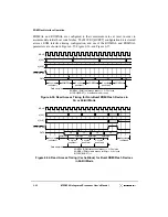
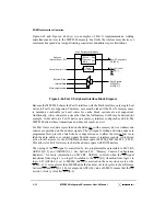
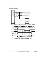
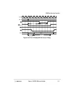
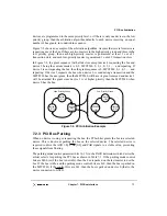
Figure 6-65 and Figure 6-66 show two examples of Port X implementations. Adding
miscellaneous devices to the MPC8240 memory bus limits the total memory devices or
maximum bus speed due to signal loading constraints and address space limitations.
Figure 6-64. Port X Peripheral Interface Block Diagram
Because the MPC8240 shares the Port X interface with the Flash interface, only single-beat
writes to Port X are supported. Therefore, care must be taken if the Port X memory space
is marked as cacheable (as burst writes for cache block castouts are not supported).
Additionally, writes of data for a size other than the full memory width may be desired (for
example, 16-bit write to a Port X device on a memory interface configured as 64-bit).The
MPC8240 allows these transactions and does not report an error.
For Port X accesses, data is provided on the data bus as with a memory device. Address and
control are provided on the address signals. The AS signal’s falling and rising edges are
programmable to provide a latch strobe or edge reference to allow the external device to
latch the data, address, or control signals from the memory interface signals. AS is driven
active for all accesses to the ROM/Flash address space (0xFF00_0000–0xFFFF_ FFFF).
This allows for Port X devices to share the address space with ROM devices.
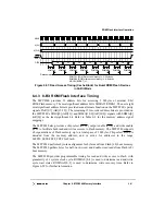
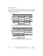
The timing of the AS signal is controlled by two programmable parameters in MCCR2,
ASFALL[0–3] and ASRISE[0–3]. See Section 4.10, “Memory Control Configuration
Registers,” for more information on MCCR2. ASFALL controls when the AS signal
transitions from a logic 1 to a logic 0 in relation to the RCS[0–1] transition from logic 1 to
logic 0. If ASFALL is set to 0b0000, the AS is asserted on the same clock cycle as the
RCS[0–1]. A value greater than 0b0000 adds that number of clock cycles to the difference
between AS and RCS[0–1]. For example, an ASFALL value of 0b0011 means that the AS
asserts 3 clock cycles after RCS[0–1].
Port X
Port X
Address
Address
Internal Bus or PCI
Port X Control
External Data
Write output enable
Central Control Unit
Port X Peripheral Interface
Port X Peripherals
Data Signals
MDH[0:31]
MDL[0:31]
Control
MUX
AR[20:0]
RCS[0:1]
AS
WE
Row
Col
Internal Data
Summary of Contents for MPC8240
Page 1: ...MPC8240UM D Rev 1 1 2001 MPC8240 Integrated Processor User s Manual ...
Page 38: ...xviii MPC8240 Integrated Processor User s Manual TABLES Table Number Title Page Number ...
Page 48: ...xlviii MPC8240 Integrated Processor User s Manual Acronyms and Abbreviations ...
Page 312: ...6 94 MPC8240 Integrated Processor User s Manual ROM Flash Interface Operation ...
Page 348: ...7 36 MPC8240 Integrated Processor User s Manual PCI Host and Agent Modes ...
Page 372: ...8 24 MPC8240 Integrated Processor User s Manual DMA Register Descriptions ...
Page 394: ...9 22 MPC8240 Integrated Processor User s Manual I2O Interface ...
Page 412: ...10 18 MPC8240 Integrated Processor User s Manual Programming Guidelines ...
Page 454: ...12 14 MPC8240 Integrated Processor User s Manual Internal Arbitration ...
Page 466: ...13 12 MPC8240 Integrated Processor User s Manual Exception Latencies ...
Page 516: ...16 14 Watchpoint Trigger Applications ...
Page 538: ...B 16 MPC8240 Integrated Processor User s Manual Setting the Endian Mode of Operation ...
Page 546: ...C 8 MPC8240 Integrated Processor User s Manual ...
Page 640: ...INDEX Index 16 MPC8240 Integrated Processor User s Manual ...

