Chapter 3. Address Maps
3-3
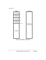
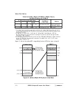
Address Map B
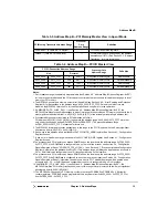
Notes:
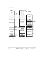
1. Part of address range is separately programmable (see Section 4.9, “Address Map B Options Register—0xE0”)
for the processor interface and the PCI interface to control whether accesses to this address range go to local
memory or PCI memory.
2. The MPC8240 generates a memory select error (if enabled; see Section 4.8.2, “Error Enabling and Detection
Registers”) for transactions in the address range 4000_0000–7FFF_FFFF. If memory select errors are
disabled, the MPC8240 returns all 1s for read operations and no update for write operations.
3. If AMBOR[CPU_FD_ALIAS_EN] = 1 (see Section 4.9, “Address Map B Options Register—0xE0”), the
MPC8240 forwards processor transactions in part of this range to the zero-based PCI memory space with the 8
most significant bits cleared (that is, AD[31:0] = 0x00 || A[8:31] of the internal peripheral logic address bus).
4. Processor addresses are translated to PCI addresses as follows:
PCI address (AD[31:0]) = 0x00 || A[8:31] to generate the address range 0000_0000–007F_FFFF. Note that
only 64 Kbytes has been defined (0xFE00_0000–0xFE00–FFFF). The processor address range
0xFE01_0000–0xFE7F_FFFF is reserved for future use.
5. The MPC8240 forwards processor transactions in this range to the PCI I/O space with the 8 most significant
bits cleared (that is, AD[31:0] = 0x00 || A[8:31]).
6. Each word in this address range is aliased to the PCI CONFIG_ADDR register. See Section 4.1, “Configuration
7. Each word in this address range is aliased to the PCI CONFIG_DATA register. See Section 4.1, “Configuration
8. The processor and PCI masters can access ROM/Flash on the local bus in the address range 0xFF00_0000–
0xFF7F_FFFF if the ROM/Flash is configured to be on the local bus at reset, see Section 2.4, “Configuration
Signals Sampled at Reset.” If PIRC2[CF_FF0_LOCAL] = 1, see Section 4.7, “Processor Interface Configuration
Registers”; otherwise, the address is sent to PCI. This address range will always be treated as an access to a
32-, or 64-bit device as configured at reset if it is configured to be on the local bus.
9. The processor and PCI masters can access ROM/Flash on the local bus in the address range 0xFF70_0000–
0xFFFF_FFFF if the ROM/Flash is configured to be on the local bus at reset (see Section 2.4, “Configuration
Signals Sampled at Reset”); otherwise, the address is sent to PCI. This address range will be treated as an
access to an 8-, 32-, or 64-bit device as configured at reset if it is configured to be on the local bus.
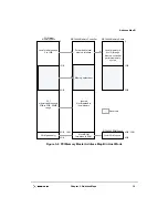
10. If AMBOR[PCI_FD_ALIAS_EN] = 1 (see Section 4.9, “Address Map B Options Register—0xE0”), the
MPC8240 forwards PCI memory transactions in part of this range to local memory with the 8 most significant
bits cleared (that is, 0x00 || AD[23:0]).
11. The MPC8240 will respond to PCI memory cycles in the range PCSRBAR to P 4 Kbytes (for
runtime registers). PCSRBAR can be programmed to be anywhere from 0x8000_0000 – 0xFCFF_FFFF or
from 0xFE00_0000 – 0xFEFF_FFFF.
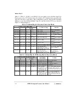
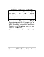
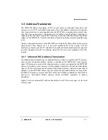
Table 3-3. Address Map B—PCI Memory Master View in Agent Mode
PCI Memory Transaction Address Range
Processor
Core
Address Range
Definition
(PCSRBAR) – (P 4 Kbytes)
—
PCI control and status registers
(LMBAR) – (LMBAR + window size)
—
Local memory space as defined by the address
translation unit (ATU). See Section 3.3, “Address
Translation,” for more information.
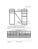
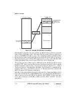
Table 3-4. Address Map B—PCI I/O Master View
PCI I/O Transaction Address Range
Processor Core
Address Range
Definition
Hex
Decimal
0000_0000
0000_FFFF
0
64K - 1
No system memory cycle
Addressable
0001_0000
007F_FFFF
64K
8M - 1
No system memory cycle
Not addressable
0080_0000
00BF_FFFF
8M
12M - 1
No system memory cycle
Addressable
00C0_0000
FFFF_FFFF
12M
4G - 1
No system memory cycle
Not addressable
Summary of Contents for MPC8240
Page 1: ...MPC8240UM D Rev 1 1 2001 MPC8240 Integrated Processor User s Manual ...
Page 38: ...xviii MPC8240 Integrated Processor User s Manual TABLES Table Number Title Page Number ...
Page 48: ...xlviii MPC8240 Integrated Processor User s Manual Acronyms and Abbreviations ...
Page 312: ...6 94 MPC8240 Integrated Processor User s Manual ROM Flash Interface Operation ...
Page 348: ...7 36 MPC8240 Integrated Processor User s Manual PCI Host and Agent Modes ...
Page 372: ...8 24 MPC8240 Integrated Processor User s Manual DMA Register Descriptions ...
Page 394: ...9 22 MPC8240 Integrated Processor User s Manual I2O Interface ...
Page 412: ...10 18 MPC8240 Integrated Processor User s Manual Programming Guidelines ...
Page 454: ...12 14 MPC8240 Integrated Processor User s Manual Internal Arbitration ...
Page 466: ...13 12 MPC8240 Integrated Processor User s Manual Exception Latencies ...
Page 516: ...16 14 Watchpoint Trigger Applications ...
Page 538: ...B 16 MPC8240 Integrated Processor User s Manual Setting the Endian Mode of Operation ...
Page 546: ...C 8 MPC8240 Integrated Processor User s Manual ...
Page 640: ...INDEX Index 16 MPC8240 Integrated Processor User s Manual ...

