Copyright © Siemens AG 2016. All rights reserved
397
ERTEC 200P-2 Manual
Technical data subject to change
Version 1.0
8
word access is permitted
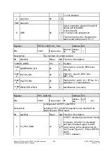
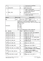
30 APB_WRITE
xh
r
h
w
0: Read access
1: Write access
31 ERR_LOCK
xh
r
h
w
Set to '1' by the HW if
erroneous SCRB access is detected.
Further HW entries are
then blocked.
The SW must reset the bit to '0' to
enable new entries.
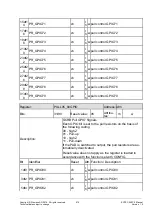
Register:
DRIVE_EMC
Address: 78h
Bits:
31dt0
Reset value:
FFFFFF
h
Attribu-
tes:
r
w
Description:
SCRB Drive Current of Dedicated Signals (1.8V)
Each GPIO bit is set to the drive current on the basis of the
following coding
-----1.8V--------
00 - 4 mA
01 - 6 mA
10 - 8 mA
11 - 12 mA
and clock enable/disable for BF and SDRAM
Bit Identifier
Reset Attr. Function / Description
1dt0 G1: DR_EMC_C
3h
r w Signal list: DTXR, XOE_DDRIVER
3dt2 G2: DR_EMC_AL
3h
r w Signal list: A14 - A0
5dt4 G3: DR_EMC_AH
3h
r w Signal list: A23 - A15
7dt6 G4: DR_EMC_DL
3h
r w
Signal list: D15 - D0, XBE0_DQM0,
XBE1_DQM1
9dt8 G5: DR_EMC_DH
3h
r w
Signal list: D31 - D16, XBE2_DQM2,
XBE3_DQM3
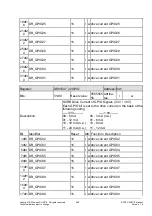
11dt1
0
G6: DR_EMC_RW
3h
r w Signal list: XWR, XRD
13dt1
2
G7: DR_EMC_PER
3h
r w Signal list: XCS_PER0 - 3
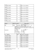
15dt1
4
G8: DR_EMC_CLK_SDRAM 3h
r w
Signal lists:CLK_O_SDRAM0,
CLK_O_SDRAM1, CLK_O_SDRAM2
17dt1
6
G9: DR_EMC_SDRAM
3h
r w
Signal list: XCS_SDRAM,
XRAS_SDRAM, XCAS_SDRAM,
XWE_SDRAM
19dt1
8
G10: DR_EMC_CLK_BF
3h
r w Signal list: CLK_O_BF0 - 2

