Copyright © Siemens AG 2016. All rights reserved
472
ERTEC 200P-2 Manual
Technical data subject to change
Version
1.0
De-
bugger
ERTEC
200+
TCK
TDI
TDO
TMS
TRST
RTCK
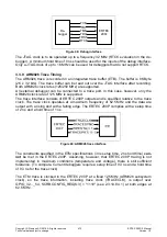
Figure 48:
Debug interface
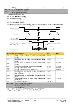
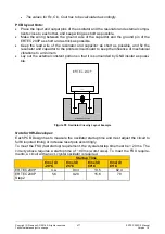
The JTAG clock is to be operated up to a frequency 32 MHz (RTCK evaluation in the de-
bugger). A minimum hold time of 0 ns should be used for the inputs of the debug interface.
Only a JTAG clock of up to 16 MHz can be used for debuggers that do not support RTCK.
3.3.9 ARM926 Trace Timing
The ARM926 trace is recorded in an integrated trace buffer (ETB). The buffer is 8 KByte
(2K x 32 bits). The trace buffer can be read out over the JTAG interface after recording.
Both ARM926 clock rates (125/250 MHz) are supported.
An external debugger can be connected to a trace port. In this case, however, only the
ARM926 clock rate of 125 MHz is supported.
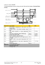
The trace interface consists of ERTEC 200P outputs and is specified relative to the trace
clock. The trace clock operates at a maximum frequency of 62.5 MHz and the data are
output with a rising and with a falling edge. The ERTEC 200P complies with a setup time
of 2 ns and a hold time of 1 ns.
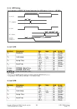
Figure 49:
ARM926 trace interface
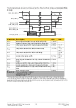
The constraints specified in the ETM specifications (3 ns setup time, 2 ns hold time)
can-
not
be met in the ERTEC 200P. Assuming, however, that ERTEC 200P tracing is not
implemented in maximum conditions (temperature and voltage), there is still sufficient
tolerance. (To compare: Current debuggers require a setup time of 0.3 ns and a hold time
of 0.3 ns for the trace clock).
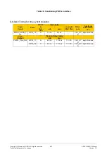
The ETM trace is clocked in the ERTEC 200P at a fixed 125 MHz (ARM926 subsystem
clock), so the trace information, including trace clock (TRACECLK), is output over
GPIO_32…_54, SCRB.CONFIG_REG(6:3) = "1110" (see 2.3.10.8.4.1) at both edges at
62.5 MHz.


