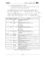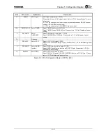
Chapter 5 Configuration Register
5-14
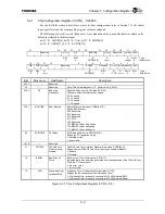
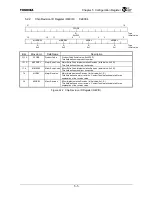
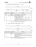
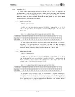
5.2.10 GBUS
Arbiter
Control Register (GARBC)
0xE02C
31
16
Reserved
:
Type
:
Initial
value
15
13
12
5
4
3 0
Reserved Reserved
Reserved
ARBMD
R/W
R/W
R/W
:
Type
0x00
1
1111
:
Initial
value
Bits Mnemonic Field
Name
Description
31:13
⎯
Reserved
⎯
12:5
⎯
Reserved
Note: This bit is always set to “0” (Initial value: 0x00, R/W).
4
⎯
Reserved
Note: This bit is always set to “1” (Initial value: 1, R/W).
3:0 ARBMD
Arbitration
Mode
Arbitration Priority (Initial value: 1111, R/W)
Specifies how to prioritize G-Bus arbitration.
0000: Fixed priority. The G-Bus arbitration priority conforms to the content of the
PRIORITY field (bits [14:0]).
1111: Round-robin (in a round-robin fashion, CHI > PDMAC > RTC > DMAC)
Others: Reserved (Don’t set these values.)
Note: Before accessing the PCI by DMAC, specify round-robin as the priority mode.
If fixed-priority mode is selected, a dead lock is likely to occur in PCI bus
access.
Figure 5.2.10 GBUS Arbiter Control Register (GARBC)
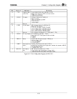
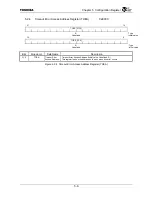
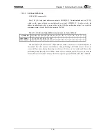
5.2.11 Register
Address
Mapping Register (RAMP)
0xE030
31
16
Reserved
:
Type
: Initial value
15
0
RAMP [31:16]
R/W
:
Type
0xFF1F
: Initial value
Bits Mnemonic Field
Name
Description
31:16
⎯
Reserved
⎯
15:0 RAMP[31:16]
Register Address
Mapping
Register Address Mapping (Initial value: 0xFF1F, R/W)
This is a base address register for the TX4925 built-in registers. It holds the high-
order 16 bits of a register address.
The default built-in register base address is 0xFFIF_0000. Even after the content of
the base address register is changed, the default value can be used to reference the
built-in registers.
(Refer to "4.2 Register Map".)
Figure 5.2.11 Register Address Mapping Register (RAMP)
Summary of Contents for TMPR4925
Page 1: ...64 Bit TX System RISC TX49 Family TMPR4925 Rev 3 0 ...
Page 4: ......
Page 15: ...Handling Precautions ...
Page 16: ......
Page 18: ...1 Using Toshiba Semiconductors Safely 1 2 ...
Page 40: ...3 General Safety Precautions and Usage Considerations 3 18 ...
Page 42: ...4 Precautions and Usage Considerations 4 2 ...
Page 43: ...TMPR4925 ...
Page 44: ......
Page 54: ...Chapter 1 Features 1 8 ...
Page 58: ...Chapter 2 Block Diagram 2 4 ...
Page 88: ...Chapter 4 Address Mapping 4 12 ...
Page 226: ...Chapter 8 DMA Controller 8 58 ...
Page 260: ...Chapter 9 SDRAM Controller 9 34 ...
Page 480: ...Chapter 15 Interrupt Controller 15 32 ...
Page 554: ...Chapter 19 Real Time Clock RTC 19 8 ...
Page 555: ...Chapter 20 Removed 20 1 20 Removed ...
Page 556: ...Chapter 20 Removed 20 2 ...
Page 564: ...Chapter 21 Extended EJTAG Interface 21 8 ...
Page 580: ...Chapter 22 Electrical Characteristics 22 16 ...
Page 588: ...Chapter 24 Usage Notes 24 2 ...


