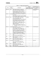
Chapter 5 Configuration Register
5-6
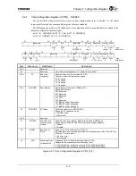
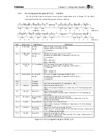
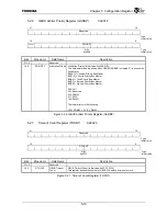
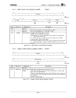
5.2.3
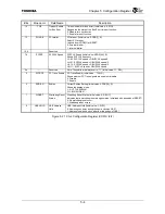
Pin Configuration Register (PCFG)
0xE008
For the bit fields whose initial values are set by boot configuration (refer to Section 3.2), the initial
input signal level and the corresponding register value are indicated.
31 30 29 28 27 26 25 23 22 21 20 19 18 17
16
SYSCLKEN
SDRCLKEN PCICLKEN
PCICLKIOEN
Reserved
Reserved SELSPI
SELCHI
SELCARD SELCE
R/W R/W
R/W R/W
R/W
R/W
R/W R/W
R/W : Type
1 1 1 ADDR[18]
ADDR[18]
0 0 0 0 0 0 0 :
Initial
value
15
14
13
12
11 9 8 7 4 3 0
SELSIOC SELSIO
ACKIN
SELTMR
SELDONE
Reserved
SELACLC SELNAND
SELDMA
R/W
R/W R/W R/W R/W
R/W
R/W R/W
: Type
0 0 0 0 1 0 0 0
0 0 0 0
: Initial value
Bits Mnemonic Field
Name
Description
31 SYSCLKEN
SYSCLK
Enable
SYSCLK Enable (Initial value: 1, R/W)
Specifies whether to output the SYSCLK.
1: Clock output.
0: L.
30
:
29 SDRCLKEN
[1
:
0]
SDRAM Clock
Enable
SDRAM Clock Enable (Initial value: 11, R/W)
Individually specifies whether to output each of SDCLK [1:0].
1: Clock output.
0: L.
Bit 30 = SDCLK [1]
Bit 29 = SDCLK [0]
28
:
27
PCICLKEN
[2
:
0]
PCI Clock Enable PCI Clock Enable (Initial value: ADDR[18], R/W)
Individually specifies whether to output each of PCICLK [2:1].
1: Clock output.
0: L.
Bit 28 = PCICLK [2]
Bit 27 = PCICLK [1]
26
PCICLKIOEN
PCI Clock I/O
Enable
PCI Clock I/O Enable (Initial value: ADDR[18], R/W)
Individually specifies whether to output each of PCICLK [2:1].
1: Clock output.
0: Clock input.
25:23
⎯
Reserved
⎯
22
⎯
Reserved
Note: This bit is always set to “0” (Initial value: 0, R/W).
21 SELSPL
Select
SPI Select SPI (Initial value: 0, R/W)
Select SPI function as PIO[23:21] pin. Please refer to “3.3 Pin Multiplexing” about
setting.
20 SELCHI
Select
CHI Select CHI (Initial value: 0, R/W)
Select SPI function as PIO[27,20:18] pin. Please refer to “3.3 Pin Multiplexing”
about setting.
19:18 SELCARD
Select PCMCIA
CARD
Select PCMCIA CARD (Initial value: 00, R/W)
Select PCMCIA CARD function as PIO[31:24] pin. Please refer to “3.3 Pin
Multiplexing” about setting.
17:16 SELCE
Select
CE[5:4]
*
Select CE[5:4]
*
(Initial value: 00, R/W)
Select CE[5:4]
*
function as PIO[29:28] pin. Please refer to “3.3 Pin Multiplexing”
about setting.
15
:
14 SELSIOC
Select SIO
Control Pins
Select SIO Control Pins (Initial value: 00, R/W)
Select SIO ch1, 0 control signals (RTS, CTS) as PIO[15,14,9,8] pin. Please refer to
“3.3 Pin Multiplexing” about setting.
13
:
12 SELSIO
Select
SIO
Select SIO (Initial value: 00, R/W)
Select SIO ch1, 0 signals (TXD, RXD) as PIO[17,16,11,10] pin. Please refer to “3.3
Pin Multiplexing” about setting.
Figure 5.2.3 Pin Configuration Register (PCFG) (1/2)
Summary of Contents for TMPR4925
Page 1: ...64 Bit TX System RISC TX49 Family TMPR4925 Rev 3 0 ...
Page 4: ......
Page 15: ...Handling Precautions ...
Page 16: ......
Page 18: ...1 Using Toshiba Semiconductors Safely 1 2 ...
Page 40: ...3 General Safety Precautions and Usage Considerations 3 18 ...
Page 42: ...4 Precautions and Usage Considerations 4 2 ...
Page 43: ...TMPR4925 ...
Page 44: ......
Page 54: ...Chapter 1 Features 1 8 ...
Page 58: ...Chapter 2 Block Diagram 2 4 ...
Page 88: ...Chapter 4 Address Mapping 4 12 ...
Page 226: ...Chapter 8 DMA Controller 8 58 ...
Page 260: ...Chapter 9 SDRAM Controller 9 34 ...
Page 480: ...Chapter 15 Interrupt Controller 15 32 ...
Page 554: ...Chapter 19 Real Time Clock RTC 19 8 ...
Page 555: ...Chapter 20 Removed 20 1 20 Removed ...
Page 556: ...Chapter 20 Removed 20 2 ...
Page 564: ...Chapter 21 Extended EJTAG Interface 21 8 ...
Page 580: ...Chapter 22 Electrical Characteristics 22 16 ...
Page 588: ...Chapter 24 Usage Notes 24 2 ...

