Chapter 12 Timer/Counter
12-10
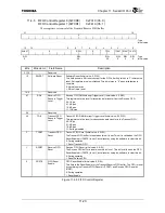
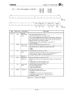
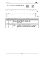
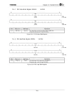
12.4.1 Timer
Control
Register
n
(TMTCRn)
TMTCR0
0xF000
TMTCR1
0xF100
TMTCR2
0xF200
31
16
0
:
Type
:
Initial
value
15 8 7 6 5 4 3 2 1 0
0 TCE
CCDE
CRE
0
ECES
CCS
TMODE
R/W
R/W
R/W
R/W
R/W R/W
:
Type
0
0
0 0
0 00 :
Initial
value
Bits Mnemonic Field
Name
Description
31:8
⎯
Reserved
⎯
7 TCE
Timer Counter
Enable
Timer Count Enable (Initial value: 0, R/W)
This field controls whether the counter runs or stops.
When in the Watchdog mode, counter operation only stops when the Watchdog
Timer Disable bit (TMWTMR2.WDIS) of the Watchdog Timer Mode Register is set.
When the Watchdog Timer Disable bit is cleared, the value of this Timer Count
Enable bit becomes “0”, but the count continues.
0: Stop counter (the counter is also cleared to “0” when CRE = 1)
1: Counter operation
6 CCDE
Counter Clock
Divider Enable
Counter Clock Divide Enable (Initial value: 0, R/W)
This bit enables the divide operation of the internal clock (IMBUSCLK). The counter
stops if this bit is set to “0” when the internal bus clock is in use.
0: Disable
1: Enable
5 CRE
Counter Reset
Enable
Counter Reset Enable (Initial value: 0, R/W)
This bit controls the counter reset when the TCE bit was used to stop the counter.
1: Stop and reset the counter to “0” when the TCE bit is cleared to “0”.
0: Only stop the counter when the TCE bit is cleared to “0”.
4
⎯
Reserved
⎯
3 ECES
External Clock
Edge Select
External Clock Edge Select (Initial value: 0, R/W)
This bit specifies the counter operation edge when using the counter input signal
(TCLK).
0: Falling edge of the counter input signal (TCLK)
1: Rising edge of the counter input signal (TCLK)
2 CCS
Counter Clock
Select
Counter Clock Select (Initial value: 0, R/W)
This bit specifies the timer clock.
0: Internal clock (IMBUSCLK)
1: External input clock (TCLK)
1:0
TMODE
Timer Mode
Timer Mode (Initial value: 00, R/W)
This bit specifies the timer operation mode.
11: Reserved
10: Watchdog Timer mode (Timer 2), Reserved (Timer 0, 1)
01: Pulse Generator mode (Timer 0, 1), Reserved (Timer 2)
00: Interval Timer mode
Figure 12.4.1 Timer Control Register
Summary of Contents for TMPR4925
Page 1: ...64 Bit TX System RISC TX49 Family TMPR4925 Rev 3 0 ...
Page 4: ......
Page 15: ...Handling Precautions ...
Page 16: ......
Page 18: ...1 Using Toshiba Semiconductors Safely 1 2 ...
Page 40: ...3 General Safety Precautions and Usage Considerations 3 18 ...
Page 42: ...4 Precautions and Usage Considerations 4 2 ...
Page 43: ...TMPR4925 ...
Page 44: ......
Page 54: ...Chapter 1 Features 1 8 ...
Page 58: ...Chapter 2 Block Diagram 2 4 ...
Page 88: ...Chapter 4 Address Mapping 4 12 ...
Page 226: ...Chapter 8 DMA Controller 8 58 ...
Page 260: ...Chapter 9 SDRAM Controller 9 34 ...
Page 480: ...Chapter 15 Interrupt Controller 15 32 ...
Page 554: ...Chapter 19 Real Time Clock RTC 19 8 ...
Page 555: ...Chapter 20 Removed 20 1 20 Removed ...
Page 556: ...Chapter 20 Removed 20 2 ...
Page 564: ...Chapter 21 Extended EJTAG Interface 21 8 ...
Page 580: ...Chapter 22 Electrical Characteristics 22 16 ...
Page 588: ...Chapter 24 Usage Notes 24 2 ...

