Chapter 9 SDRAM Controller
9-13
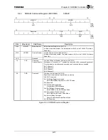
9.4.1
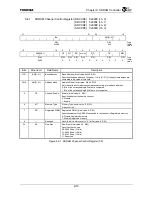
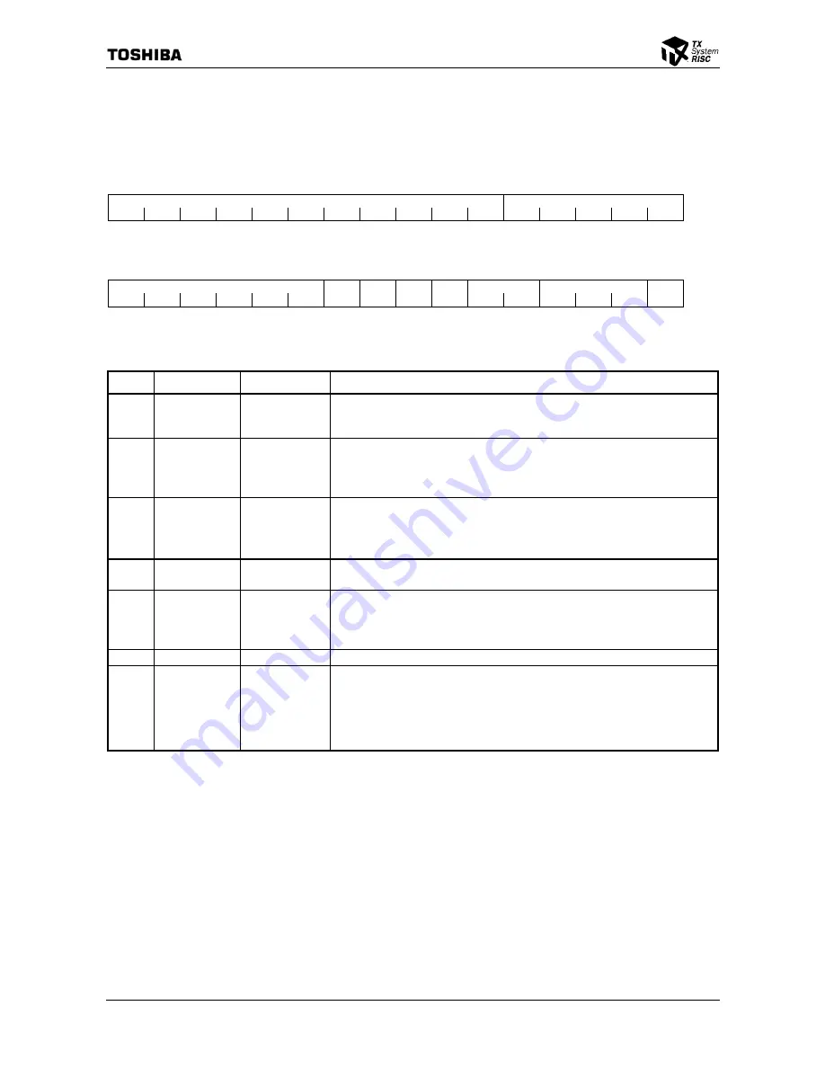
SDRAM Channel Control Register (SDCCR0) 0x8000 (ch. 0)
(SDCCR1) 0x8004 (ch. 1)
(SDCCR2) 0x8008 (ch. 2)
(SDCCR3)
0x800C
(ch.
3)
31
21
20
16
BA
AM[31:27]
R/W
R/W
:
Type
0x000
0x0
: Initial
value
15 10 9 8 7 6 5 4 3 2 1 0
AM[26:21] CE
MT
RD
Reserved
RS CS
MW
R/W
R/W R/W R/W R/W
R/W
R/W
R/W
:
Type
0x00
0 0 0 0 0 0 0 0 0 0
: Initial
value
Bits Mnemonic Field
Name
Description
31:21
BA[31:21]
Base Address
Base Address (Initial value: 0x000, R/W)
Specifies the base address. The upper 11 bits [31:21] of the physical address are
compared to the value of this field.
20:10
AM[31:21]
Address Mask
Address Mask (Initial value: 0x000, R/W)
Sets the valid bits for address comparison according to the base address.
0: Bits of the corresponding BA field are compared.
1: Bits of the corresponding BA field are not compared.
9
CE
Channel Enable
Enable (Initial value: 0, R/W)
Specifies whether to enable a channel.
0: Disable
1: Enable
8
MT
Memory Type
Memory Type (Initial value: 0, R/W)
Always set to 0.
7
RD
Registered DIMM Registered DIMM (Initial value: 0, R/W)
Specifies whether the SDRAM connected to the channel is Registered memory.
0: Disable Registered memory
1: Enable Registered memory
6
⎯
Reserved
Note: this bit is always set to “0” (Initial value: 0, R/W)
5:4
RS
Row Size
Row Size (Initial value: 00, R/W)
Specifies the row size.
00: 2048 Rows (11 bits)
01: 4096 Rows (12 bits)
10: 8192 Rows (13 bits)
11: Reserved
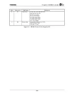
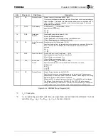
Figure 9.4.1 SDRAM Channel Control Register (1/2)
Summary of Contents for TMPR4925
Page 1: ...64 Bit TX System RISC TX49 Family TMPR4925 Rev 3 0 ...
Page 4: ......
Page 15: ...Handling Precautions ...
Page 16: ......
Page 18: ...1 Using Toshiba Semiconductors Safely 1 2 ...
Page 40: ...3 General Safety Precautions and Usage Considerations 3 18 ...
Page 42: ...4 Precautions and Usage Considerations 4 2 ...
Page 43: ...TMPR4925 ...
Page 44: ......
Page 54: ...Chapter 1 Features 1 8 ...
Page 58: ...Chapter 2 Block Diagram 2 4 ...
Page 88: ...Chapter 4 Address Mapping 4 12 ...
Page 226: ...Chapter 8 DMA Controller 8 58 ...
Page 260: ...Chapter 9 SDRAM Controller 9 34 ...
Page 480: ...Chapter 15 Interrupt Controller 15 32 ...
Page 554: ...Chapter 19 Real Time Clock RTC 19 8 ...
Page 555: ...Chapter 20 Removed 20 1 20 Removed ...
Page 556: ...Chapter 20 Removed 20 2 ...
Page 564: ...Chapter 21 Extended EJTAG Interface 21 8 ...
Page 580: ...Chapter 22 Electrical Characteristics 22 16 ...
Page 588: ...Chapter 24 Usage Notes 24 2 ...


