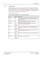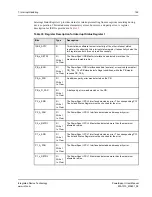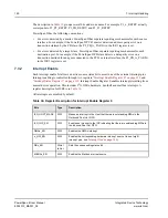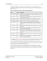
7. Interrupt Handling
153
PowerSpan II User Manual
80A1010_MA001_09
Integrated Device Technology
www.idt.com
7.4
Interrupt Pins
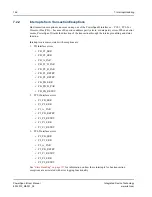
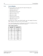
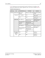
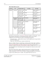
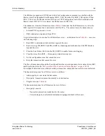
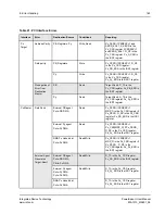
PowerSpan II has the following interrupt pins:
•
P1_INTA#
•
P2_INTA#
•
INT[5:0]_
Pins INT[5:0]_ are 5V tolerant and general purpose interrupt pins. Interrupt pins are active low and,
when configured as input, are sampled on three successive processor bus clock edges to ensure
appropriate setting of a status bit.
Each pin is bidirectional, open drain, active low and level sensitive. The input/output character of each
interrupt pin is controlled through a corresponding bit in the
“Interrupt Direction Register” on
. Each pin can be configured as either an input or output. All pins are configured as inputs by
default.
P1_INTA# and P2_INTA# are intended to be used with PCI interfaces PCI-1 and PCI-2. They are
electrically PCI compliant. To configure PCI interface Px with interrupt capability, the following
register settings are required:
•
INT_PIN = 0x01, in the
“PCI-1 Miscellaneous 1 Register” on page 262
(Px_MISC1). This setting
enables a single function PCI device INTA#
•
Px_HW_DIR = 0x01, in the
“Interrupt Direction Register” on page 347
(ID). Px_INTA# is
configured as an output pin.
If the PCI interface Px does not require interrupt capability, the following register settings are
necessary:
•
INT_PIN = 0x00, in the Px_MISC1 register. This setting enables a single function PCI device that
is using no interrupts.
•
Px_INTA = user defined, in the ID register. Px_INTA# is used as general purpose pin.
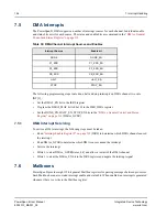
PowerSpan II provides an EEPROM load feature to automatically control the interrupt capabilities of
PCI-1 and PCI-2 (see
).

