X20 system modules • Analog input modules • X20AI2222
X20 system User's Manual 3.10
147
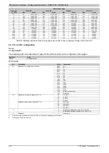
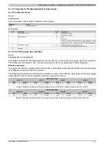
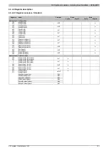
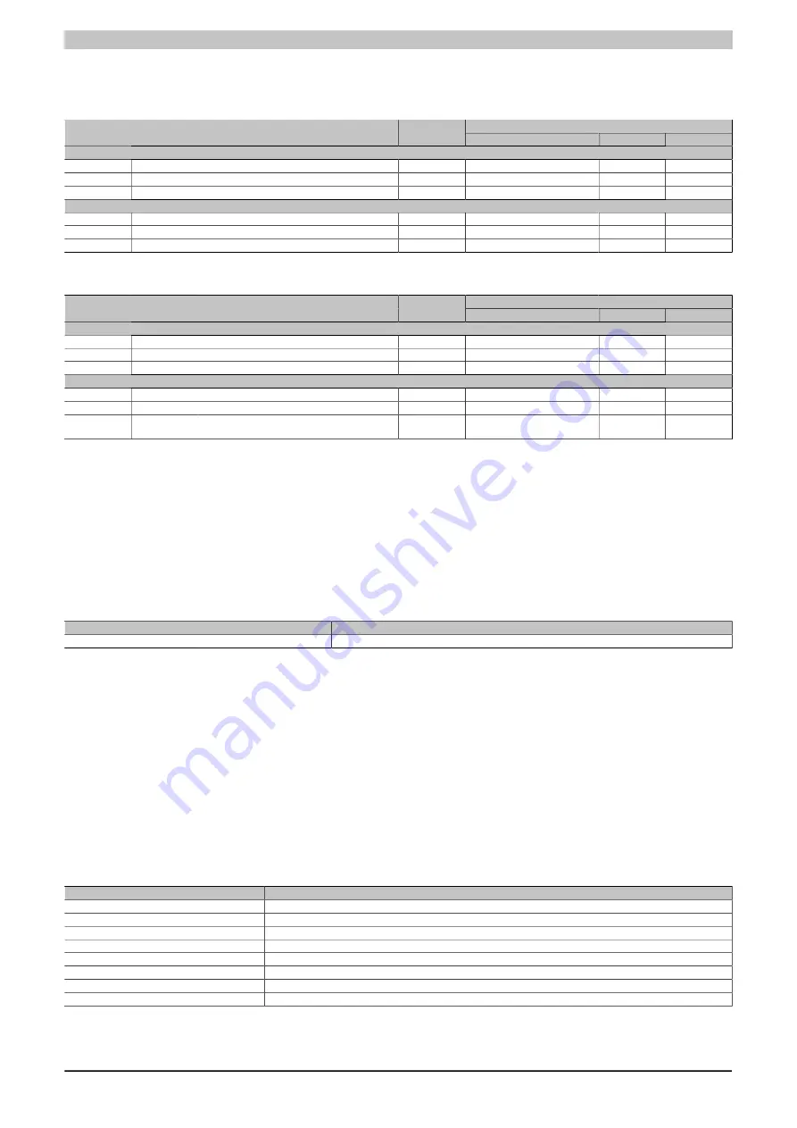
4.3.3.8 Register description
4.3.3.8.1 Function model 0 - Standard
Read
Write
Register
Name
Data type
Cyclic
Non-cyclic
Cyclic
Non-cyclic
Analog signal - Configuration
16
USINT
●
20
INT
●
22
INT
●
Analog signal - Communication
0
INT
●
2
INT
●
30
USINT
●
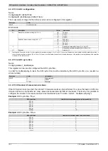
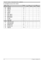
4.3.3.8.2 Function model 254 - Bus controller
Read
Write
Register
Offset
1)
Name
Data type
Cyclic
Non-cyclic
Cyclic
Non-cyclic
Analog signal - Configuration
16
-
USINT
●
20
-
INT
●
22
-
INT
●
Analog signal - Communication
0
0
INT
●
2
2
INT
●
30
-
USINT
●
1)
The offset specifies the position of the register within the CAN object.
4.3.3.8.3 Analog inputs
The input state is collected with a fixed offset to the network cycle and transferred in the same cycle.
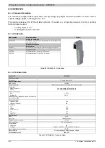
4.3.3.8.4 Analog input values
Name:
AnalogInput01 to AnalogInput02
The analog input values are mapped to this register.
Data type
Value
Input signal:
INT
-32,768 to 32,767
Voltage signal -10 to 10 VDC
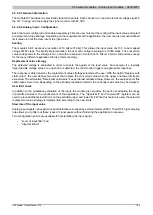
4.3.3.8.5 Input filter
This module is equipped with a configurable input filter. The minimum cycle time must be >500 μs. Filtering is
disabled for shorter cycle times.
If the input filter is active, then the scan rate for the channels is measured in ms. The time offset between the
channels is 200 μs. The conversion takes place asynchronously to the network cycle.
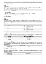
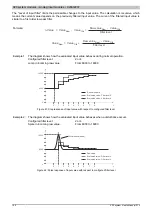
4.3.3.8.5.1 Input ramp limitation
Input ramp limitation can only take place when a filter is used; the input ramp is limited before filtering takes place.
The amount the input value changes is checked to make sure that specified limits are not exceeded. If the values
are exceeded, the adjusted input value is equal to the old value ± the limit value.
Configurable limit values:
Value
Limit value
0
The input value is used without limitation.
1
0x3FFF = 16383
2
0x1FFF = 8191
3
0x0FFF = 4095
4
0x07FF = 2047
5
0x03FF = 1023
6
0x01FF = 511
7
0x00FF = 255
Summary of Contents for X20 System
Page 2: ......


