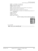
0x3
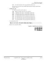
Way 3
0x4
-
0x7
Unused
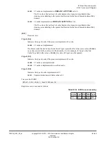
L1 D-data RAM
0x0
Way0-Bank0
0x1
Way0-Bank1
0x2
Way1-Bank0
0x3
Way1-Bank1
...
0x7
Way3-Bank1
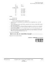
[17:12]
Reserved,
RES0
.
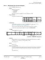
RAM address, [11:0]
Indicates the index address of the first memory error.
• A fatal error results in the RAMID, Way, and RAM address recording the fatal error, even if the
sticky bit is set.
• Only L1 Data data and L1 Data dirty RAMs can signal fatal errors, because all other RAM instances
are protected only by parity.
• If two or more memory errors in the same RAM occur in the same cycle, only one error is reported.
• If two or more first memory error events from different RAMs occur in the same cycle, one of the
errors is selected arbitrarily.
• If two or more memory error events from different RAMs, that do not match the RAMID, Way, and
index information in this register while the sticky Valid bit is set, occur in the same cycle, then the
Other error count field is incremented only by one.
To access the CPUMERRSR:
MRRC p15, 2, <Rt>, <Rt2>, c15; Read CPUMERRSR into Rt and Rt2
MCRR p15, 2, <Rt>, <Rt2>, c15; Write Rt and Rt2 to CPUMERRSR
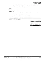
Register access is encoded as follows:
Table B1-38 CPUMERRSR access encoding
coproc opc1 CRm
1111
0010 1111
B1 AArch32 system registers
B1.44 CPU Memory Error Syndrome Register
100236_0100_00_en
Copyright © 2015–2017, 2019 Arm Limited or its affiliates. All rights
reserved.
B1-216
Non-Confidential
Summary of Contents for Cortex-A35
Page 4: ......
Page 18: ......
Page 26: ......
Page 27: ...Part A Functional Description ...
Page 28: ......
Page 145: ...Part B Register Descriptions ...
Page 146: ......
Page 573: ...Part C Debug ...
Page 574: ......
Page 845: ...Part D Appendices ...
Page 846: ......


