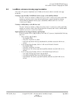
A.15
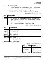
APB interface signals
The debug APB bus supports clock, reset, addressing, and data handling signals when the processor
includes an APB interface to provide access to the debug and performance monitoring registers.
You must balance all APB interface signals with respect to
CLKIN
and time them relative to
PCLKENDBG
.
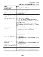
Table A-43 APB interface signals
Signal
Direction Description
nPRESETDBG
Input
APB reset, active-LOW:
0
Apply reset to APB interface.
1
Do not apply reset to APB interface.
PADDRDBG[21:2]
Input
APB address bus.
PADDRDBG31
Input
APB address bus bit[31]:
0
Not an external debugger access.
1
External debugger access.
PCLKENDBG
Input
APB clock enable.
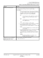
PENABLEDBG
Input
Indicates the second and subsequent cycles of an APB transfer.
PRDATADBG[31:0]
Output
APB read data.
PREADYDBG
Output
APB slave ready.
An APB slave can deassert
PREADYDBG
to extend a transfer by inserting wait states.
PSELDBG
Input
Debug bus access.
PSLVERRDBG
Output
APB slave transfer error:
0
No transfer error.
1
Transfer error.
PWDATADBG[31:0]
Input
APB write data.
PWRITEDBG
Input
APB read or write signal:
0
Reads from APB.
1
Writes to APB.
A Signal Descriptions
A.15 APB interface signals
100236_0100_00_en
Copyright © 2015–2017, 2019 Arm Limited or its affiliates. All rights
reserved.
Appx-A-873
Non-Confidential
Summary of Contents for Cortex-A35
Page 4: ......
Page 18: ......
Page 26: ......
Page 27: ...Part A Functional Description ...
Page 28: ......
Page 145: ...Part B Register Descriptions ...
Page 146: ......
Page 573: ...Part C Debug ...
Page 574: ......
Page 845: ...Part D Appendices ...
Page 846: ......

