B1.117 TTBR1 with Short-descriptor translation table format
TTBR1 has a specific format when using the Short-descriptor translation table format. TTBCR.EAE
determines which format of the register is in use.
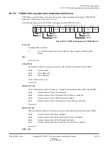
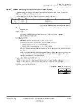
The following figure shows the TTBR1 bit assignments when TTBCR.EAE is 0.
31
0
1
2
3
4
5
6
7
IRGN[1]
S
RES
0
NOS
TTB1
IRGN[0]
RGN
Figure B1-65 TTBR1 bit assignments, TTBCR.EAE is 0
TTB1, [31:7]
Translation table base 1 address, bits[31:x], where x is 14-(TTBCR.N). Bits [x-1:7] are
RES0
.
The translation table must be aligned on a 16KByte boundary.
If bits [x-1:7] are not all zero, this is a misaligned Translation Table Base Address. Its effects are
CONSTRAINED UNPREDICTABLE
, where bits [x-1:7] are treated as if all the bits are zero. The value
read back from those bits is the value written.
IRGN[0], [6]
See IRGN[1] below for description of the IRGN field.
NOS, [5]
Not Outer Shareable bit. Indicates the Outer Shareable attribute for the memory associated with
a translation table walk that has the Shareable attribute, indicated by TTBR0.S is 1. The possible
values are:
0
Outer Shareable.
1
Inner Shareable.
This bit is ignored when TTBR0.S is 0.
RGN, [4:3]
Region bits. Indicates the Outer cacheability attributes for the memory associated with the
translation table walks. The possible values are:
0b00
Normal memory, Outer Non-cacheable.
0b01
Normal memory, Outer Write-Back Write-Allocate Cacheable.
0b10
Normal memory, Outer Write-Through Cacheable.
0b11
Normal memory, Outer Write-Back no Write-Allocate Cacheable.
IMP, [2]
Reserved,
RES0
.
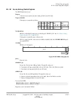
S, [1]
Shareable bit. Indicates the Shareable attribute for the memory associated with the translation
table walks. The possible values are:
0
Non-shareable.
1
Shareable.
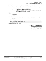
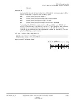
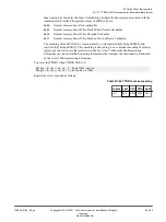
IRGN[1], [0]
B1 AArch32 system registers
B1.117 TTBR1 with Short-descriptor translation table format
100236_0100_00_en
Copyright © 2015–2017, 2019 Arm Limited or its affiliates. All rights
reserved.
B1-351
Non-Confidential
Summary of Contents for Cortex-A35
Page 4: ......
Page 18: ......
Page 26: ......
Page 27: ...Part A Functional Description ...
Page 28: ......
Page 145: ...Part B Register Descriptions ...
Page 146: ......
Page 573: ...Part C Debug ...
Page 574: ......
Page 845: ...Part D Appendices ...
Page 846: ......

