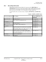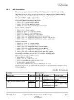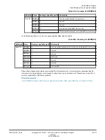
L2 cache
Data cache lines are allocated to the L2 cache only when evicted from the L1 memory system,
not when first fetched from the system. The only exceptions to this rule are for memory marked
with the inner transient hint, or for non-temporal loads that are only ever allocated to the L2
cache. The L1 cache can prefetch data from the system, without data being evicted from the L2
cache.
Instruction cache lines are allocated to the L2 cache when fetched from the system and can be
invalidated during maintenance operations.
The L2 cache is 8-way set associative. The L2 cache tags are looked up in parallel with the SCU
duplicate tags. If both the L2 tag and SCU duplicate tag hit, a read accesses the L2 cache in
preference to snooping one of the other cores.
L2 RAMs are invalidated automatically at reset unless the
L2RSTDISABLE
signal is set HIGH
when the
nL2RESET
signal is deasserted.
Further features of the L2 cache are:
• Configurable size of 128KB, 256KB, 512KB, and 1MB.
• Fixed line length of 64 bytes.
• Physically indexed and tagged.
• Optional ECC protection.
• A pseudo-LRU replacement policy.
ACP
Optional 128-bit wide I/O coherent ACP interface that can allocate to the L2 cache.
Master memory interface
The SCU connects the cores to the external memory system through a 128-bit-wide master
memory interface that uses ACE, CHI, or AXI technology. The memory interface supports
integer ratios of the processor clock period up to and including 1:1 and a 40-bit physical address
range.
The L2 memory system has two abort mechanisms, a synchronous one and an asynchronous one.
Related information
A7.5 Handling of external aborts
on page A7-103
Chapter A9 ACE Master Interface
Chapter A10 CHI Master Interface
Chapter A8 AXI Master Interface
Chapter A11 ACP Slave Interface
on page A11-135
A7 L2 Memory System
A7.1 About the L2 memory system
100236_0100_00_en
Copyright © 2015–2017, 2019 Arm Limited or its affiliates. All rights
reserved.
A7-99
Non-Confidential
Summary of Contents for Cortex-A35
Page 4: ......
Page 18: ......
Page 26: ......
Page 27: ...Part A Functional Description ...
Page 28: ......
Page 145: ...Part B Register Descriptions ...
Page 146: ......
Page 573: ...Part C Debug ...
Page 574: ......
Page 845: ...Part D Appendices ...
Page 846: ......

