ISD94100 Series Technical Reference Manual
Sep 9, 2019
Page
188
of 928
Rev1.09
IS
D
9
410
0
S
ER
IE
S
T
E
C
HN
ICA
L
RE
F
E
RE
NCE
M
AN
U
AL
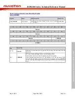
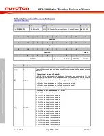
PD Standby Power-down Wake-up Control Register
(CLK_PDSWKCTL)
Register
Offset
R/W Description
Reset Value
CLK_PDSWKCTL
0xAC
R/W GPD Standby Power-down Wakeup Control Register
0x0000_0000
31
30
29
28
27
26
25
24
Reserved
23
22
21
20
19
18
17
16
Reserved
15
14
13
12
11
10
9
8
Reserved
DBEN
7
6
5
4
3
2
1
0
WKPSEL
Reserved
PFWKEN
PRWKEN
WKEN
Bits
Description
[31:9]
Reserved
Reserved. Any values read should be ignored. When writing to this field always write with
reset value.
[8]
DBEN
PD Input Signal De-bounce Enable Bit
The DBEN bit is used to enable the de-bounce function for each corresponding I/O. If the
input signal pulse width cannot be sampled by continuous two de-bounce sample cycle, the
input signal transition is seen as the signal bounce and will not trigger the wakeup. The de-
bounce clock source is the internal low speed RC oscillator.
0 = Standby power-down wake-up pin De-bounce function disable.
1 = Standby power-down wake-up pin De-bounce function enable.
The de-bounce function is valid only for edge triggered.
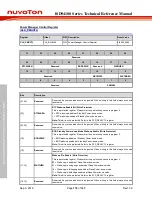
[7:4]
WKPSEL
PD Standby Power-down Wake-up Pin Select
0000 = PD.0 wake-up function enabled.
0001 = PD.1 wake-up function enabled.
0010 = PD.2 wake-up function enabled.
0011 = PD.3 wake-up function enabled.
0100 = PD.4 wake-up function enabled.
0101 = PD.5 wake-up function enabled.
0110 = PD.6 wake-up function enabled.
0111 = PD.7 wake-up function enabled.
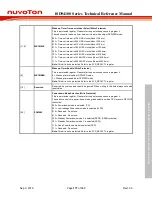
1000 = PD.8 wake-up function enabled.
1001 = PD.9 wake-up function enabled.
1010 = PD.10 wake-up function enabled.
1011 = PD.11 wake-up function enabled.
1100 = PD.12 wake-up function enabled.
1101 = PD.13 wake-up function enabled.
1110 = PD.14 wake-up function enabled.


