ISD94100 Series Technical Reference Manual
Sep 9, 2019
Page
250
of 928
Rev1.09
IS
D
9
410
0
S
ER
IE
S
T
E
C
HN
ICA
L
RE
F
E
RE
NCE
M
AN
U
AL
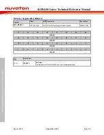
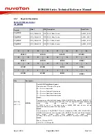
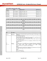
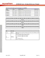
Port A-D Data Output Value (Px_DOUT)
Register
Offset
R/W Description
Reset Value
PA_DOUT
0x008
R/W PA Data Output Value
0x0000_FXFF
PB_DOUT
0x048
R/W PB Data Output Value
0x0000_F3FF
PC_DOUT
0x088
R/W PC Data Output Value
0x0000_FFFF
PD_DOUT
0x0C8
R/W PD Data Output Value
0x0000_FFFF
31
30
29
28
27
26
25
24
Reserved
23
22
21
20
19
18
17
16
Reserved
15
14
13
12
11
10
9
8
DOUT
7
6
5
4
3
2
1
0
DOUT
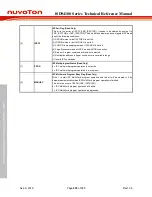
Bits
Description
[31:16]
Reserved
Reserved. Any values read should be ignored. When writing to this field always write with
reset value.
[n]
n=0,1..15
DOUT[n]
Port A-D Pin[n] Output Value
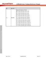
Each of these bits controls the status of a Px.n pin when the Px.n is configured as Push-
pull output, Open-drain output or Quasi-bidirectional mode.
0 = Px.n will drive Low if the Px.n pin is configured as Push-pull output, Open-drain output
or Quasi-bidirectional mode.
1 = Px.n will drive High if the Px.n pin is configured as Push-pull output or Quasi-
bidirectional mode.
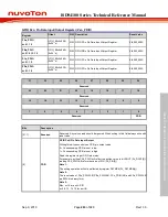
Note 1:
The reset value of PA_DOUT[8] field is defined by GPA8_LOW (CONFIG0[11]).
If GPA8_LOW is set to 0, the reset value of PA_DOUT[8] is 0 and PA.8 pin will be drive
low state after chip power-on or reset period.
If GPA8_LOW is set to 1, the reset value of PA_DOUT[8] is 1.
Note 2:
The reset value of PA_DOUT[11:8] is 111Xb in binary form, the reset value of PA_DOUT[8]
is based on the setting of GPA_LOW (CONFIG0[11]).
Note 3:
Max. n=15 for port A/C/D
n=0..9, 13, 14, 15 for port B

