ISD94100 Series Technical Reference Manual
Sep 9, 2019
Page
448
of 928
Rev1.09
IS
D
9
410
0
S
ER
IE
S
T
E
C
HN
ICA
L
RE
F
E
RE
NCE
M
AN
U
AL
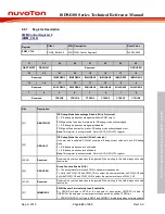
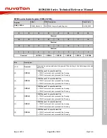
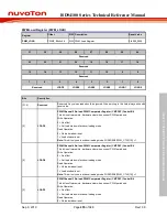
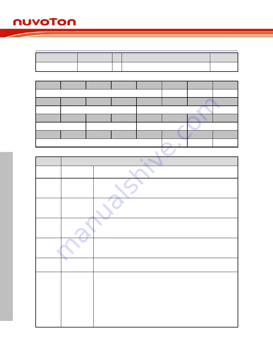
PWM Synchronization Register (PWM_SYNC)
Register
Offset
R/W Description
Reset Value
PWM_SYNC
0x08
R/W PWM Synchronization Register
0x0000_0000
31
30
29
28
27
26
25
24
Reserved
PHSDIR4
PHSDIR2
PHSDIR0
23
22
21
20
19
18
17
16
SINPINV
SFLTCNT
SFLTCSEL
SNFLTEN
15
14
13
12
11
10
9
8
Reserved
SINSRC4
SINSRC2
SINSRC0
7
6
5
4
3
2
1
0
Reserved
PHSEN4
PHSEN2
PHSEN0
Bits
Description
[31:27]
Reserved
Reserved. Any values read should be ignored. When writing to this field always write with
reset value.
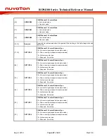
[26]
PHSDIR4
PWM Channel 4 Phase Direction Control
0 = Control PWM counter count decrement after synchronizing.
1 = Control PWM counter count increment after synchronizing.
[25]
PHSDIR2
PWM Channel 2 Phase Direction Control
0 = Control PWM counter count decrement after synchronizing.
1 = Control PWM counter count increment after synchronizing.
[24]
PHSDIR0
PWM Channel 0 Phase Direction Control
0 = Control PWM counter count decrement after synchronizing.
1 = Control PWM counter count increment after synchronizing.
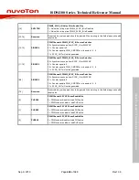
[23]
SINPINV
SYNC Input Pin Inverse
0 = The state of pin SYNC is passed to the negative edge detector.
1 = The inversed state of pin SYNC is passed to the negative edge detector.
[22:20]
SFLTCNT
SYNC Edge Detector Filter Count
The register bits control the counter number of edge detector.
[19:17]
SFLTCSEL
SYNC Edge Detector Filter Clock Selection
000 = Filter clock = HCLK.
001 = Filter clock = HCLK/2.
010 = Filter clock = HCLK/4.
011 = Filter clock = HCLK/8.
100 = Filter clock = HCLK/16.
101 = Filter clock = HCLK/32.
110 = Filter clock = HCLK/64.
111 = Filter clock = HCLK/128.

