ISD94100 Series Technical Reference Manual
Sep 9, 2019
Page
263
of 928
Rev1.09
IS
D
9
410
0
S
ER
IE
S
T
E
C
HN
ICA
L
RE
F
E
RE
NCE
M
AN
U
AL
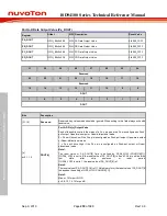
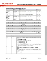
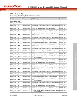
GPIO Px.n Pin Data Input/Output Register (Pxn_PDIO)
Register
Offset
R/W Description
Reset Value
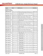
PAn_PDIO
n=0,1..15
0x800+
(0x04 * n)
R/W GPIO PA.n Pin Data Input/Output Register
0x0000_000X
PBn_PDIO
n=0,1..9,13..15
0x840+
(0x04 * n)
R/W GPIO PB.n Pin Data Input/Output Register
0x0000_000X
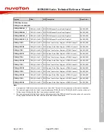
PCn_PDIO
n=0,1..15
0x880+
(0x04 * n)
R/W GPIO PC.n Pin Data Input/Output Register
0x0000_000X
PDn_PDIO
n=0,1..15
0x8C0+
(0x04 * n)
R/W GPIO PD.n Pin Data Input/Output Register
0x0000_000X
31
30
29
28
27
26
25
24
Reserved
23
22
21
20
19
18
17
16
Reserved
15
14
13
12
11
10
9
8
Reserved
7
6
5
4
3
2
1
0
Reserved
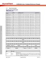
PDIO
Bits
Description
[31:1]
Reserved
Reserved. Any values read should be ignored. When writing to this field always write with
reset value.
[0]
PDIO
GPIO Px.N Pin Data Input/Output
Writing this bit can control one GPIO pin output value.
0 = Corresponding GPIO pin set to low.
1 = Corresponding GPIO pin set to high.
Read this register to get GPIO pin status.
For example, writing PA0_PDIO will reflect the written value to bit DOUT (Px_DOUT[0]),
reading PA0_PDIO will return the value of PIN (PA_PIN[0]).
Note 1:
The writing operation will not be affected by register DATMSK (Px_DATMSK[n]).
Note 2:
The reset value of PAn_PDIO[3:0], PBn_PDIO[3:0], PCn_PDIO[3:0] and PDn_PDIO[3:0]
are 000Xb in binary form.
Note 3:
Max. n=15 for port A/C/D
n=0..9, 13, 14, 15 for port B


