ISD94100 Series Technical Reference Manual
Sep 9, 2019
Page
874
of 928
Rev1.09
IS
D
9
410
0
S
ER
IE
S
T
E
C
HN
ICA
L
RE
F
E
RE
NCE
M
AN
U
AL
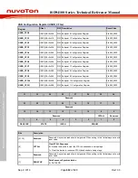
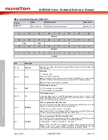
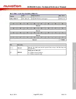
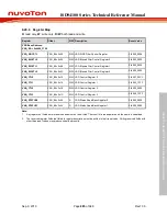
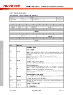
DMIC Clock Divider Register (DMIC_DIV)
Register
Offset
R/W Description
Reset Value
DMIC_DIV
0x04
R/W DMIC Clock Divider Register
0x0000_0307
31
30
29
28
27
26
25
24
Reserved
23
22
21
20
19
18
17
16
FCLR
THIE
TH
15
14
13
12
11
10
9
8
MCLKDIV
7
6
5
4
3
2
1
0
PCLKDIV
Bits
Description
[31:24]
Reserved
Reserved. Any values read should be ignored. When writing to this field always write
with reset value.
[23:22]
FCLR
FIFO Clear
11 = Clear the FIFO.
Others = Reserved. Do not use.
Note 1:
To clear the FIFO, need to write FCLR (DMIC_DIV[23:22]) to 11b, and can read
the EMPTY (DMIC_STATUS[1]) bit to make sure that the FIFO has been cleared.
Note 2:
This field is auto cleared by hardware.
[21]
THIE
FIFO Threshold Interrupt
0 = FIFO threshold interrupt Disabled
1 = FIFO threshold interrupt Enabled.
[20:16]
TH
FIFO Threshold Level
If the valid data count of the FIFO data buffer is more than or equal to TH
(DMIC_DIV[20:16]) setting, the THIF (DMIC_STATUS[2]) bit will set to 1, else the THIF
(DMIC_STATUS[2]) bit will be cleared to 0.
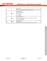
[15:8]
MCLKDIV
Divider to generate the DMIC Bus Clock
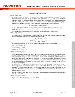
The value in this field is the frequency divider for generating the DMIC bus clock. The
frequency is obtained according to the following equation.
F_DMIC_CLK = (F_DMIC_MCLK)/(1 + MCLKDIV)
where F_DMIC_MCLK is the frequency of DMIC working main clock (DMIC_MCLK) and
F_DMIC_CLK is the frequency of DMIC bus clock (DMIC_CLK).
[7:0]
PCLKDIV
Divider to generate the DMIC Working Main Clock
The value in this field is the frequency divider for generating the DMIC working main
clock. The frequency is obtained according to the following equation.
F_DMIC_MCLK = (F_DMIC_CLK_SRC)/(1 + PCLKDIV)
where F_DMIC_CLK_SRC is the frequency of DMIC module clock source, which is
defined in the clock control register DMICSEL (CLK_CLKSEL2[11:10]) and
F_DMIC_MCLK is the frequency of DMIC working main clock (DMIC_MCLK).

