ISD94100 Series Technical Reference Manual
Sep 9, 2019
Page
730
of 928
Rev1.09
IS
D
9
410
0
S
ER
IE
S
T
E
C
HN
ICA
L
RE
F
E
RE
NCE
M
AN
U
AL
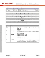
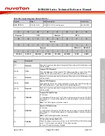
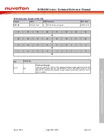
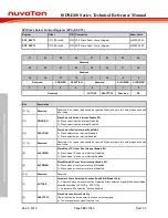
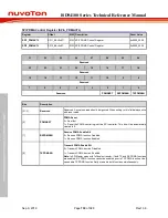
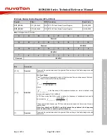
SPI PDMA Control Register (SPIn_PDMACTL)
Register
Offset
R/W Description
Reset Value
SPI1_PDMACTL
0x0C
R/W SPI1 PDMA Control Register
0x0000_0000
SPI2_PDMACTL
0x0C
R/W SPI2 PDMA Control Register
0x0000_0000
31
30
29
28
27
26
25
24
Reserved
23
22
21
20
19
18
17
16
Reserved
15
14
13
12
11
10
9
8
Reserved
7
6
5
4
3
2
1
0
Reserved
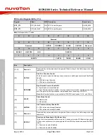
PDMARST
RXPDMAEN
TXPDMAEN
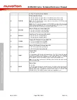
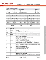
Bits
Description
[31:3]
Reserved
Reserved. Any values read should be ignored. When writing to this field always write
with reset value.
[2]
PDMARST
PDMA Reset
0 = No effect.
1 = Reset the PDMA control logic of the SPI controller. This bit will be automatically
cleared to 0.
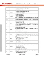
[1]
RXPDMAEN
Receive PDMA Enable Bit
0 = Receive PDMA function Disabled.
1 = Receive PDMA function Enabled.
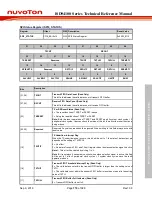
[0]
TXPDMAEN
Transmit PDMA Enable Bit
0 = Transmit PDMA function Disabled.
1 = Transmit PDMA function Enabled.
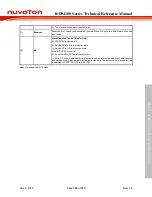
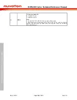
Note:
In SPI Master mode with full duplex transfer, if both TX and RX PDMA functions
are enabled, RX PDMA function cannot be enabled prior to TX PDMA function. User
can enable TX PDMA function firstly or enable both functions simultaneously.

