ISD94100 Series Technical Reference Manual
Sep 9, 2019
Page
218
of 928
Rev1.09
IS
D
9
410
0
S
ER
IE
S
T
E
C
HN
ICA
L
RE
F
E
RE
NCE
M
AN
U
AL
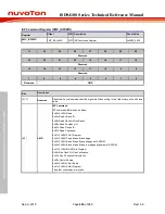
[20]
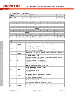
CBORST
Brown-Out Reset Enable Bit
0 = Brown-out reset Enabled after power on.
1 = Brown-out reset Disabled after power on.
[19]
CBODEN
Brown-Out Detector Enable Bit
0 = Brown-out detect Enabled after powered on.
1 = Brown-out detect Disabled after power on.
[18:12]
Reserved
Reserved bit should always be programmed with 1.
[11]
GPA8_LOW
Initial State of GPA8 Selection
0 = GPA8 is low after chip power on or reset.
1 = GPA8 follows CIOINI.
[10]
CIOINI
I/O Initial State Selection
0 = All GPIO set as Quasi-bidirectional mode after chip power on.
1 = All GPIO set as input tri-state mode after power on.
[9:8]
Reserved
Reserved bit should always be programmed with 1.
[7:6]
CBS
Chip Booting Selection
When CBS[0] = 0, the LDROM base address is mapping to 0x100000 and APROM base
address is mapping to 0x0. User could access both APROM and LDROM without boot
switching. In other words, if IAP mode is supported, the code in LDROM and APROM can
be called by each other.
00 = Boot from LDROM with IAP mode.
01 = Boot from LDROM without IAP mode.
10 = Boot from APROM with IAP mode.
11 = Boot from APROM without IAP mode.
Note:
BS (FMC_ISPCTL[1]) is only be used to control boot switching when CBS[0] = 1.
VECMAP (FMC_ISPSTS[23:9]) is only be used to remap 0x0~0x1ff when CBS[0] = 0.
[5]
Reserved
Reserved bit should always be programmed with 1.
[4:3]
CWDTEN
Watchdog Timer Hardware Enable Bit
When watchdog timer hardware enable function is enabled, the watchdog enable bit
WDTEN (WDT_CTL[7]) and watchdog reset enable bit RSTEN (WDT_CTL[1]) is set to 1
automatically after power on. The clock source of watchdog timer is force at LIRC and LIRC
can’t be disable.
CWDTEN[2:0]
is CONFIG0[31][4][3],
111 = WDT hardware enable function is inactive.
Others = WDT hardware enable function is active. WDT clock is always on.
[2]
LOCK2
Security Lock Control 2
0 = ICE interface is disabled.
1 = ICE operation not restricted except by LOCK (CONFIG0[1]) bit.
[1]
LOCK
Security Lock Control
0 = Flash memory content is locked.
1 = Flash memory content is not locked. When flash data is locked by LOCK, the only
operation permissible on flash memory is mass erase ensuring that APROM cannot be read
or configuration changed before APROM erased. LOCK will disable: Read from FLASH,
Program FLASH, Page ERASE flash (APROM or CONFIG), write SRAM, access to DMA
registers.


