ISD94100 Series Technical Reference Manual
Sep 9, 2019
Page
738
of 928
Rev1.09
IS
D
9
410
0
S
ER
IE
S
T
E
C
HN
ICA
L
RE
F
E
RE
NCE
M
AN
U
AL
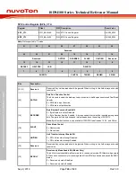
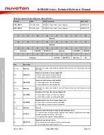
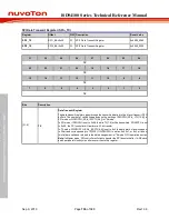
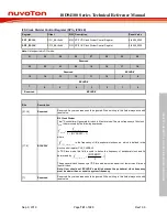
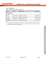
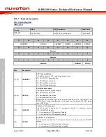
I2S Control Register (SPIn_I2SCTL)
Register
Offset
R/W Description
Reset Value
SPI1_I2SCTL
0x60
R/W SP1 I2S Control Register
0x0000_0000
SPI2_I2SCTL
0x60
R/W SPI2 I2S Control Register
0x0000_0000
Note:
Not supported in SPI mode.
31
30
29
28
27
26
25
24
Reserved
FORMAT
Reserved
LZCIEN
RZCIEN
23
22
21
20
19
18
17
16
RXLCH
Reserved
FLZCDEN
FRZCDEN
15
14
13
12
11
10
9
8
MCLKEN
Reserved
SLAVE
7
6
5
4
3
2
1
0
ORDER
MONO
WDWIDTH
MUTE
RXEN
TXEN
I2SEN
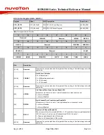
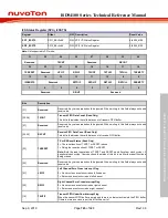
Bits
Description
[31:30]
Reserved
Reserved. Any values read should be ignored. When writing to this field always write with
reset value.
[29:28]
FORMAT
Data Format Selection
00 = I
2
S data format.
01 = MSB justified data format.
10 = PCM mode A.
11 = PCM mode B.
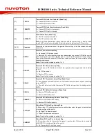
[27:26]
Reserved
Reserved. Any values read should be ignored. When writing to this field always write with
reset value.
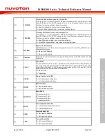
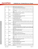
[25]
LZCIEN
Left Channel Zero Cross Interrupt Enable Bit
Interrupt occurs if this bit is set to 1 and left channel zero cross event occurs.
0 = Interrupt Disabled.
1 = Interrupt Enabled.
[24]
RZCIEN
Right Channel Zero Cross Interrupt Enable Bit
Interrupt occurs if this bit is set to 1 and right channel zero cross event occurs.
0 = Interrupt Disabled.
1 = Interrupt Enabled.
[23]
RXLCH
Receive Left Channel Enable Bit
When monaural format is selected (MONO = 1), I
2
S controller will receive right channel data
if RXLCH is set to 0, and receive left channel data if RXLCH is set to 1.
0 = Receive right channel data in Mono mode.
1 = Receive left channel data in Mono mode.
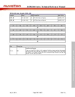
[22:18]
Reserved
Reserved. Any values read should be ignored. When writing to this field always write with
reset value.

