ISD94100 Series Technical Reference Manual
Sep 9, 2019
Page
727
of 928
Rev1.09
IS
D
9
410
0
S
ER
IE
S
T
E
C
HN
ICA
L
RE
F
E
RE
NCE
M
AN
U
AL
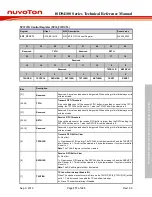
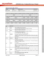
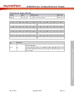
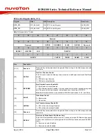
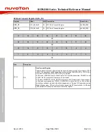
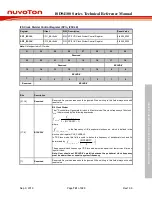
SPI Clock Divider Register (SPIn_CLKDIV)
Register
Offset
R/W Description
Reset Value
SPI1_CLKDIV
0x04
R/W SPI1 Clock Divider Register
0x0000_0000
SPI2_CLKDIV
0x04
R/W SPI2 Clock Divider Register
0x0000_0000
31
30
29
28
27
26
25
24
Reserved
23
22
21
20
19
18
17
16
Reserved
15
14
13
12
11
10
9
8
Reserved
DIVIDER
7
6
5
4
3
2
1
0
DIVIDER
Bits
Description
[31:9]
Reserved
Reserved. Any values read should be ignored. When writing to this field always write with
reset value.
[8:0]
DIVIDER
Clock Divider
The value in this field is the frequency divider for generating the peripheral clock, f
spi_eclk
, and
the SPI bus clock of SPI Master. The frequency is obtained according to the following
equation.
)
1
(
_
_
_
+
=
DIVIDER
f
f
src
clock
spi
eclk
spi
where
f
src
clock
spi
_
_
is the peripheral clock source, which is defined in the clock control
register, CLK_CLKSEL2.
Note1:
Not supported in I
2
S mode.
Note2:
User should set DIVIDER carefully because the peripheral clock frequency must be
slower than or equal to system frequency.


