ISD94100 Series Technical Reference Manual
Sep 9, 2019
Page
201
of 928
Rev1.09
IS
D
9
410
0
S
ER
IE
S
T
E
C
HN
ICA
L
RE
F
E
RE
NCE
M
AN
U
AL
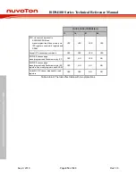
FMC_MPDAT0~FMC_MPDAT3 :
N/A
0x0000_0008
FMC_ISPDAT: Unique ID Word 2
FMC_MPDAT0~FMC_MPDAT3 :
N/A
Vector Remap
0x2E
Valid address in APROM,LDROM or boot loader
It must be 512 bytes alignment
N/A
Table 6.4.4-3 ISP Command List
ISP Procedure
The FMC controller supports flash memory read, erase and re-programming functions. Some
control bits or ISP registers are write-protected, and require unlock and lock sequence before and
after access. Refer to Register Description section for detailed information.
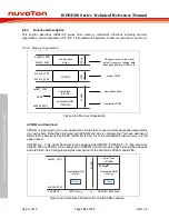
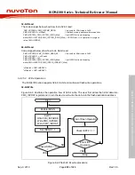
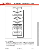
Figure 6.4-8 illustrates the ISP flow:
Configure FMC_ISPCTL register to decide to which part of flash memory to update: LDROM,
APROM or configuration bytes. Writing 1 to ISPEN (FMC_ISPCTL[0]) enables ISP module.
Configure FMC_ISPCMD (for ISP command) and FMC_ISPDAT (read/write data) registers to make
device ready for a specific ISP operation.
Enable ISPEN
Set ISPGO = 1
End of ISP
Operation
?
(Read FMC_ISPDAT)
&
Check ISPFF = 1?
YES
End of Flash
Operation
NO
(Set PT)
Write FMC_ISPADDR
Write FMC_ISPCMD
(Write FMC_ISPDAT )
Check ISPGO = 0
?
NO
YES
Start
Stop
Figure 6.4-8 ISP Procedure Example
Writing 1 to ISPGO bit (FMC_ISPTRG[0]) starts the ISP function. The ISPGO (FMC_ISPTRG[0]) bit
is self-cleared when ISP function finishes.
When the ISPGO (FMC_ISPTRG[0]) bit is set, CPU will wait for ISP operation to finish during this


