ISD94100 Series Technical Reference Manual
Sep 9, 2019
Page
841
of 928
Rev1.09
IS
D
9
410
0
S
ER
IE
S
T
E
C
HN
ICA
L
RE
F
E
RE
NCE
M
AN
U
AL
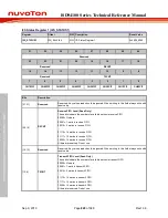
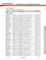
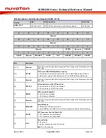
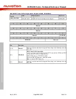
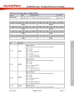
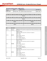
Register
Offset
R/W Description
Reset Value
USBD Base Address:
USBD_BA = 0x400C_0000
Register
USBD_BUFSEG10
0x5A0
R/W Endpoint 10 Buffer Segmentation Register
0x0000_0000
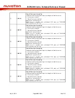
USBD_MXPLD10
0x5A4
R/W Endpoint 10 Maximal Payload Register
0x0000_0000
USBD_CFG10
0x5A8
R/W Endpoint 10 Configuration Register
0x0000_0000
USBD_CFGP10
0x5AC
R/W
Endpoint 10 Set Stall and Clear In/Out Ready Control
Register
0x0000_0000
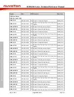
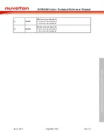
USBD_BUFSEG11
0x5B0
R/W Endpoint 11 Buffer Segmentation Register
0x0000_0000
USBD_MXPLD11
0x5B4
R/W Endpoint 11 Maximal Payload Register
0x0000_0000
USBD_CFG11
0x5B8
R/W Endpoint 11 Configuration Register
0x0000_0000
USBD_CFGP11
0x5BC
R/W
Endpoint 11 Set Stall and Clear In/Out Ready Control
Register
0x0000_0000
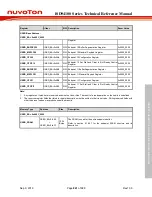
Note:
1.
Any register not listed here is reserved and must not be written. The result of a read operation on these bits is undefined.
2.
The reserved register fields that listed in register description must be written to their reset value. Writing reserved fields with
other than reset values may produce undefined results.
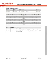
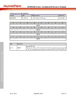
Memory Type
Address
Size
Description
USBD_BA = 0x400C_0000
USBD_SRAM
0x100
~
0x4FF
1024
Bytes
The SRAM is used for the entire endpoints buffer.
Refer to section 6.18.5.7 for the endpoint SRAM structure and its
description.


