ISD94100 Series Technical Reference Manual
Sep 9, 2019
Page
344
of 928
Rev1.09
IS
D
9
410
0
S
ER
IE
S
T
E
C
HN
ICA
L
RE
F
E
RE
NCE
M
AN
U
AL
Prescale
TMx
(PWMx_CH0)
Pulse
Generator
Output
Control
TMx_EXT
(PWMx_CH1)
TMRx_PWMCLK
i
Comparator
Counter
a
Interrupt
Generator
Trigger
Generator
NVIC
ADC
Trigger events
Interrupt events
t
i
a
i
t
denotes interrupt events
denotes trigger events
denotes interrupt, trigger and pulse generate events
Note:
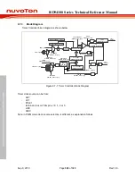
Figure 6.7-7 PWM Complementary Mode Architecture Diagram
6.7.4
Basic Configuration
Typically software needs to configure the registers below to configure a timer:
FUNCSEL bit (TIMERx_ALTCTL[0]) chooses timer or PWM function for a timer,
TMRxCKEN is the timer enable bit,
TMRxSEL bits select the timer clock source,
x=0, 1, 2 or 3.
For example,
-
FUNCSEL (TIMER1_ALTCTL[0]) = 0 chooses timer fucntion for Timer0,
-
FUNCSEL (TIMER1_ALTCTL[0]) = 1 chooses PWM function for Timer0,
-
TMR0CKEN (CLK_APBCLK0[2]) is the Timer0 enable/disable bit
-
and TMR0SEL (CLK_CLKSEL1[10:8]) chooses the Timer0 clock source.
6.7.4.1 TIMER01 basic configurations
Clock source configuration
–
Enable TIMER0 peripheral clock in TMR0CKEN (CLK_APBCLK0[2]).
–
Enable TIMER1 peripheral clock in TMR1CKEN (CLK_APBCLK0[3]).
Reset configuration
–
Reset TIMER0 controller in TMR0RST (SYS_IPRST1[2]).
–
Reset TIMER1 controller in TMR1RST (SYS_IPRST1[3]).
Pin configuration
Group
Pin Name
GPIO
MFP
TM0
PA.11
MFP2


