ISD94100 Series Technical Reference Manual
Sep 9, 2019
Page
712
of 928
Rev1.09
IS
D
9
410
0
S
ER
IE
S
T
E
C
HN
ICA
L
RE
F
E
RE
NCE
M
AN
U
AL
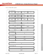
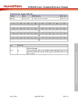
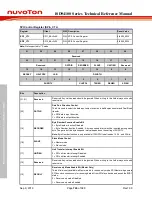
[2]
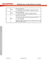
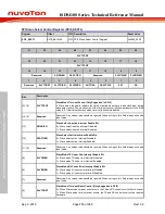
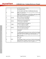
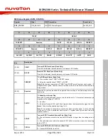
TXNEG
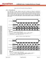
Transmit on Negative Edge
0 = Transmitted data output signal is changed on the rising edge of SPI bus clock.
1 = Transmitted data output signal is changed on the falling edge of SPI bus clock.
[1]
RXNEG
Receive on Negative Edge
0 = Received data input signal is latched on the rising edge of SPI bus clock.
1 = Received data input signal is latched on the falling edge of SPI bus clock.
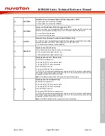
[0]
SPIEN
SPI Transfer Control Enable Bit
In Master mode, the transfer will start when there is data in the FIFO buffer after this bit is
set to 1. In Slave mode, this device is ready to receive data when this bit is set to 1.
0 = Transfer control Disabled.
1 = Transfer control Enabled.
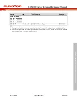
Note:
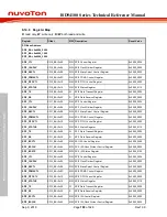
Before changing the configurations of SPI0_CTL, SPI0_CLKDIV, SPI0_SSCTL and
SPI0_FIFOCTL registers, user shall clear the SPIEN (SPI0_CTL[0]) and confirm the
SPIENSTS (SPI0_STATUS[15]) is 0.


